鑫景福致力于滿足“快速服務,零缺陷,輔助研發”PCBA訂購單需求。


PCBA加工
This artICle will discuss what rigid-flex PCBs, the advantages of using them, and the rules for designing applications using them.
In electronics, we sometiMES encounter new technologies that seem to originate from the past. Rigid-flex PCB technology dates back about 50 years and required the replacement of wiring harnesses in spacecraft. The first commercial mobile computer (a little over 25 pounds!) used rigid-flex technology.
Today, laptops, wearable technology, Medical Equipment, test equipment, and satellites are just a few of the applications that rely on rigid-flex PCBs.
What is a rigid-flex PCB?
For rigid-flex PCBs, the flexible circuit substrate and the rigid circuit substrate are laminated together. Rigid-flex PCBs straddle the boundaries of traditional rigid PCBs and the unique properties of flexible circuits lithographically etched onto flexible insulating films using highly ductile electrodeposited or roll-anneaLED copper conductors.
Flexible circuits include laminates made of flexible polyimide such as Kapton or Norton, and copper laminated together by heat, acrylic adhesive, and pressure.
As with traditional PCBs, you can mount components on both sides of a rigid board. Rigid-flex designs do not use connectors or connecting cables between sections because integration occurs between rigid and flexible circuits. Instead, flex circuits electrically connect the system together.
Several things can be accomplished without connectors and connecting cables:
1.Improve the ability of circuits to transmit signals losslessly
2.Adapt to controlled impedance
3.Eliminate connection issues such as cold splices
4.reduce weight
5.Free up space for other components
Each rigid-flex PCB is divided into regions with different materials and different numbers of layers. Rigid regions may have more layers than flexible regions, and the material transitions from FR-4 to polyimide in the transition region.
Complex designs often go from rigid to flexible and back to rigid multiple times. As these intersections occur, the overlap of rigid-flex materials requires keeping the holes away from the transition zone to maintain integrity. Additionally, many rigid-flex designs include stainless steel or aluminum reinforcements to provide additional support for connectors and components.
For more information on flex PCBs, check out our article on flex and rigid-flex PCBs for project design.
Different design rules apply to rigid-flex PCB design
Different challenges offset the versatility and flexibility that allows you to build 3D designs and products. Traditional rigid-flex PCB designs allow you to mount your product's components, connectors, and chassis to the physically stronger, rigid portion of the component. Also, with traditional designs, flex circuits are used only as interconnects, while reducing mass and improving vibration resistance.
New product designs combined with improved flex circuit technology have introduced new design rules for rigid-flex PCBs. Your design team is now free to place components on the flex circuit area. Combining this degree of freedom with a multi-layered approach to rigid-flex design allows you and your team to build more circuits in your design. However, gaining this freedom adds some challenges in routing and vias.
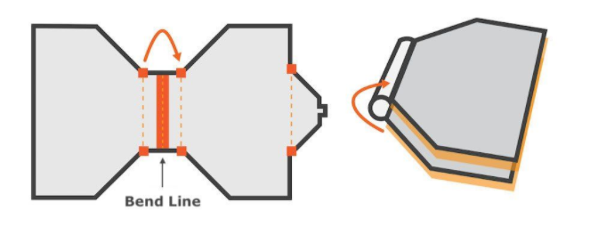
Flex circuits always have bent wires that affect wiring. You cannot place components or vias close to bend lines due to potential material stress.
Rendering demonstrates the basic concepts of rigid-flex PCB bend lines.
Even when components are positioned correctly, bent flex circuits can create repetitive mechanical stress on surface mount pads and vias. Your team can reduce these stresses by using through-hole plating and securing the pads with additional overlays to reinforce the pad support.
When designing trace routing, follow practices to reduce circuit stress. Use shaded polygons to maintain flexibility when carrying power or ground planes on flex circuits. You should use curved traces instead of 90° or 45° angles, and use a teardrop pattern to vary the trace width.

Teardrop pattern for trace-to-trace connections.
These practices reduce stress points and weaknesses. Another best practice is to distribute stress across the traces by staggering the top and bottom traces of a double-sided flex circuit. Offset traces prevent traces from overlapping each other in the same direction and strengthen the PCB.
You should also route perpendicular to the flex line to reduce stress. When going from rigid to flexible and back to rigid, the number of layers may vary from one medium to another. You can use traces to increase the stiffness of the flex circuit by offsetting the routing of adjacent layers.
Electromechanical factors affect design
When you design a rigid-flex PCB, consider the electromechanical factors that affect flex circuits and rigid boards. When building your design, pay attention to the ratio of bend radius to thickness. For flexible circuits, tight bends or increased thickness in the flex area can increase the chance of failure. Manufacturers recommend keeping the bend radius at least ten times the thickness of the flex circuit material and building a "paper doll" of the circuit to determine where the bend occurs.
You should avoid stretching the flex circuit along the outer bend or compressing it along the inner bend. Increasing the bend angle beyond 90° increases tension at one point and compression at another point on the flex circuit.
Another key issue for rigid-flex reliability is the thickness and type of conductors in the flex region. You can reduce thickness and mechanical stress by reducing the amount of plating on the conductors and using pad-only plating. Using thick copper, gold or nickel plating reduces flexibility in bends and allows mechanical stress and fracture to occur.
Rigid-flex PCB design requires teamwork
New PCB design tools enable your design team to manage multi-layer stacks, visualize 3D electromechanical designs, check design rules, and SIMulate the operation of flex circuits. Even with these tools at hand, the successful design of rigid-flex PCBs depends on teamwork between your team and the manufacturer.
Teamwork must start at the earliest stages of a project, continue throughout the design process, and depend on consistent communication
Kingford SMT chip processing capability
10-19,2022


抖音二維碼

Q Q二維碼

微信二維碼
點擊
然后
聯系
然后
聯系
電話熱線
13410863085Q Q

微信

- 郵箱