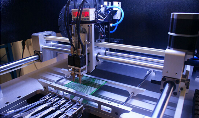
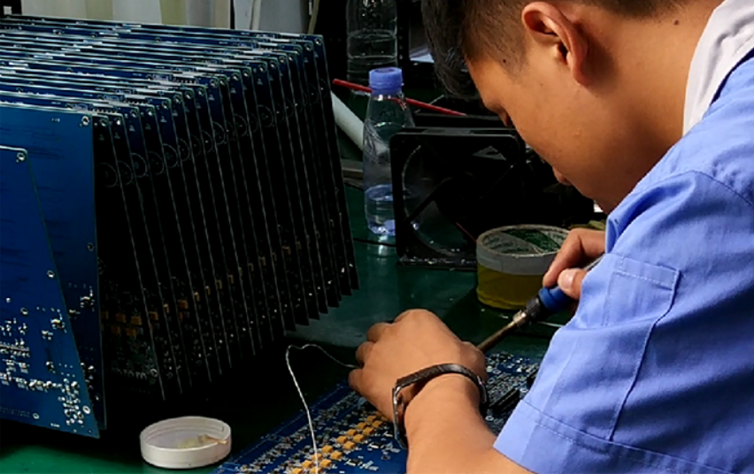
鑫景福致力于滿足“快速服務,零缺陷,輔助研發”PCBA訂購單需求。


PCBA加工
The PCB processing manufacturers always have various undesirable phenomena in the process of circuit board welding. Here are 15 common undesirable analyses in the process of circuit board welding.
1、 There are many dirty PCB boards left after welding:
1. FLUX has high solid content and too much non-volatile matter.
2. Preheating is not conducted before welding or the preheating temperature is too low (the time is too short for immersion welding).
3. The walking speed is too fast (FLUX fails to volatilize fully).
4. The temperature of tin furnace is not enough.

5. There are too many impurities in the tin furnace or the degree of tin is low.
6. It is caused by adding anti-oxidation agent or anti-oxidation oil.
7. Too much flux is applied.
8. There are too many cutouts or open components on the PCB, so there is no preheating.
9. The element foot and plate hole are out of proportion (the hole is too large), whICh makes the flux rise.
10. PCB itself has precoated rosin.
11. In tin lining process, FLUX has strong wettability.
12. PCB process problem, too few vias, resulting in poor volatilization of FLUX.
13. The angle of PCB entering tin solution is not correct during manual immersion.
14. During the use of FLUX, diluent was not added for a long time.
2、 Fire:
1. The flash point of flux is too low, and no flame retardant is added.
2. There is no air knife, resulting in too much flux coating, which drops onto the heating pipe during preheating.
3. The angle of the air knife is not correct (so that the flux is not evenly coated on the PCB).
4. There are too many adhesive strips on the PCB, which ignites the adhesive strips.
5. There is too much flux on the PCB and it drops onto the heating tube.
6. The walking speed is too fast (FLUX is not completely volatilized, and the FLUX drops) or too slow (causing too high heat temperature on the board surface).
7. The preheating temperature is too high.
8. Process problems (poor PCB board, heat pipe too close to PCB).
3、 Corrosion (components turn green and solder joints turn black)
1. Copper reacts with FLUX to form green copper compounds.
2. Lead tin reacts with FLUX to form a black lead tin compound.
3. Inadequate preheating (low preheating temperature and fast moving speed) results in too many residues of FLUX and too many residues of harmful substances).
4. Residues absorb water (conductivity of water-soluble substances is not up to standard)
5. FLUX to be cleaned is used, and it is not cleaned or timely cleaned after welding.
6. FLUX activity is too strong.
7. The electronIC components react with the active substances in FLUX.
4、 Electric connection and leakage (poor insulation)
1. FLUX forms ion residues on the board; Or FLUX residual water absorption, water absorption and conductivity.
2. The PCB design is unreasonable and the wiring is too close.
3. The quality of PCB solder mask is poor and conductive easily.
5、 Missing weld, faulty weld, continuous weld
1. Insufficient FLUX activity.
2. The wettability of FLUX is not enough.
3. The amount of FLUX coating is too SMAll.
4. The FLUX coating is uneven.
5. The PCB area cannot be painted with FLUX.
6. PCB area is free of tin.
7. Some pads or weld legs are severely oxidized.
8. The PCB wiring is unreasonable (the distribution of components is unreasonable).
9. The walking board is not in the right direction.
10. Tin content is insufficient or copper exceeds the standard; [The melting point (liquidus) of molten tin increases due to impurities exceeding the standard]
11. The foam tube is blocked and the foam is uneven, causing uneven coating of FLUX on PCB.
12. The setting of air knife is unreasonable (FLUX is not blown evenly).
13. The walking speed and preheating are not well matched.
14. Improper operation method during manual tin DIPping.
15. The chain inclination is unreasonable.
16. The wave crest is uneven.
6、 The solder joint is too bright or not bright
1. FLUX problem: A. It can be changed by changing the additives (FLUX selection problem); B. FLUX is slightly corroded.
2. Poor tin (such as too low tin content).
7、 Short circuit
1. Short circuit caused by molten tin:
A. Continuous welding occurred but was not detected.
B. The tin liquid does not reach the normal operating temperature, and there is a "tin wire" bridge between solder joints.
C. There are fine solder beads between solder joints.
D. When continuous welding occurs, the bridge is erected.
2. Problems with FLUX:
A. FLUX has low activity and poor wettability, resulting in tin bonding between solder joints.
B. The absolute impedance of FLUX is not enough, resulting in short connection between solder joints.
3. PCB problems: for example, the solder mask of PCB itself falls off, causing short circuit
8、 Big smoke and strong taste:
1. Problems with FLUX itself
A. Resin: if ordinary resin is used, the smoke is large
B. Solvent: here it refers to the SMEll or pungent smell of solvent used by FLUX may be large
C. Activator: heavy smoke and pungent smell
2. Incomplete exhaust system
9、 Splash, tin bead:
1. Flux
A. The water content in FLUX is large (or exceeds the standard)
B. High boiling point components in FLUX (not fully volatilized after preheating)
2. Process
A. Low preheating temperature (FLUX solvent is not completely volatilized)
B. Fast walking speed does not reach the preheating effect
C. The chain inclination is not good, there are bubbles between the tin liquid and PCB, and tin beads are produced after the bubbles burst
D. The amount of FLUX coating is too large (no air knife or bad air knife)
E. Improper operation during manual tin dipping
F. Wet working environment
3. Problems with PCB boards
A. The board surface is wet and not completely preheated, or there is moisture
B. Unreasonable hole design for PCB gas leakage, resulting in air entrapment between PCB and molten tin
C. The PCB design is unreasonable, and the pins of parts are too dense, causing cavitation
D. Poor PCB through hole
10、 Poor tin coating and insufficient solder joints
1. FLUX has poor wettability
2. FLUX has weak activity
3. The wetting or activation temperature is low and the flooding is too small
4. The double wave process is used, and the effective components in FLUX have been completely volatilized during a tin pass
5. If the preheating temperature is too high, the activator will activate in advance. When the tin wave passes, the activator will have no activity, or the activity will be very weak;
6. The walking speed is too slow, which makes the preheating temperature too high
7. The FLUX coating is uneven.
8. Soldering pads and component pins are severely oxidized, resulting in poor tin eating
9. Too little FLUX coating; PCB pads and component pins are not completely wetted
10. Unreasonable PCB design; The Layout of components on PCB is unreasonable, which affects the tin coating of some components
11、 FLUX foaming is not good
1. Incorrect FLUX selection
2. The foam tube hole is too large (generally speaking, the foam tube hole of the wash free FLUX is smaller, and the foam tube hole of the resin FLUX is larger)
3. The foaming area of the foaming tank is too large
4. Air pressure of air pump is too low
5. The foaming tube has the condition that the tube hole leaks or blocks the air hole, resulting in uneven foaming
6. Excessive diluent addition
12、 Too much foaming
1. Air pressure is too high
2. The foaming area is too small
3. Excess FLUX added in the weld support groove
4. Diluent was not added in time, resulting in high FLUX concentration
13、 FLUX Discoloration
Some opaque FLUX are added with a small amount of photosensitive additives, which will change color when exposed to light, but will not affect the welding effect and performance of FLUX
14、 PCB solder mask falls off, peels off or bubbles
1. More than 80% of the reasons are problems in PCB manufacturing
A. Not clean
B. Poor solder mask
C. PCB board and solder mask do not match
D. Dirt in the drill hole enters the solder mask
E. Too many tiMES of tin passing during hot air leveling
2. Some additives in FLUX can destroy the solder mask
3. Tin liquid temperature or preheating temperature is too high
4. Too many times of welding
5. During manual tin dipping operation, PCB stays on the surface of tin solution for too long
15、 Electric signal changes at high frequency
1. FLUX has low insulation resistance and poor insulation
2. The residual is uneven, the insulation resistance is uneven, and capacitance or resistance can be formed on the circuit.
3. The water extraction rate of FLUX is unqualified
4. The above problems may not occur when used in the cleaning process (or the situation can be solved by cleaning)


抖音二維碼

Q Q二維碼

微信二維碼
點擊
然后
聯系
然后
聯系
電話熱線
13410863085Q Q

微信

- 郵箱