鑫景福致力于滿足“快速服務,零缺陷,輔助研發(fā)”PCBA訂購單需求。


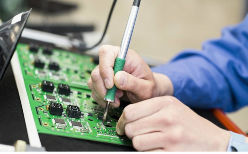
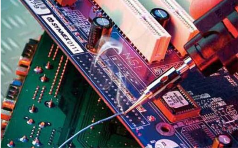
PCBA加工
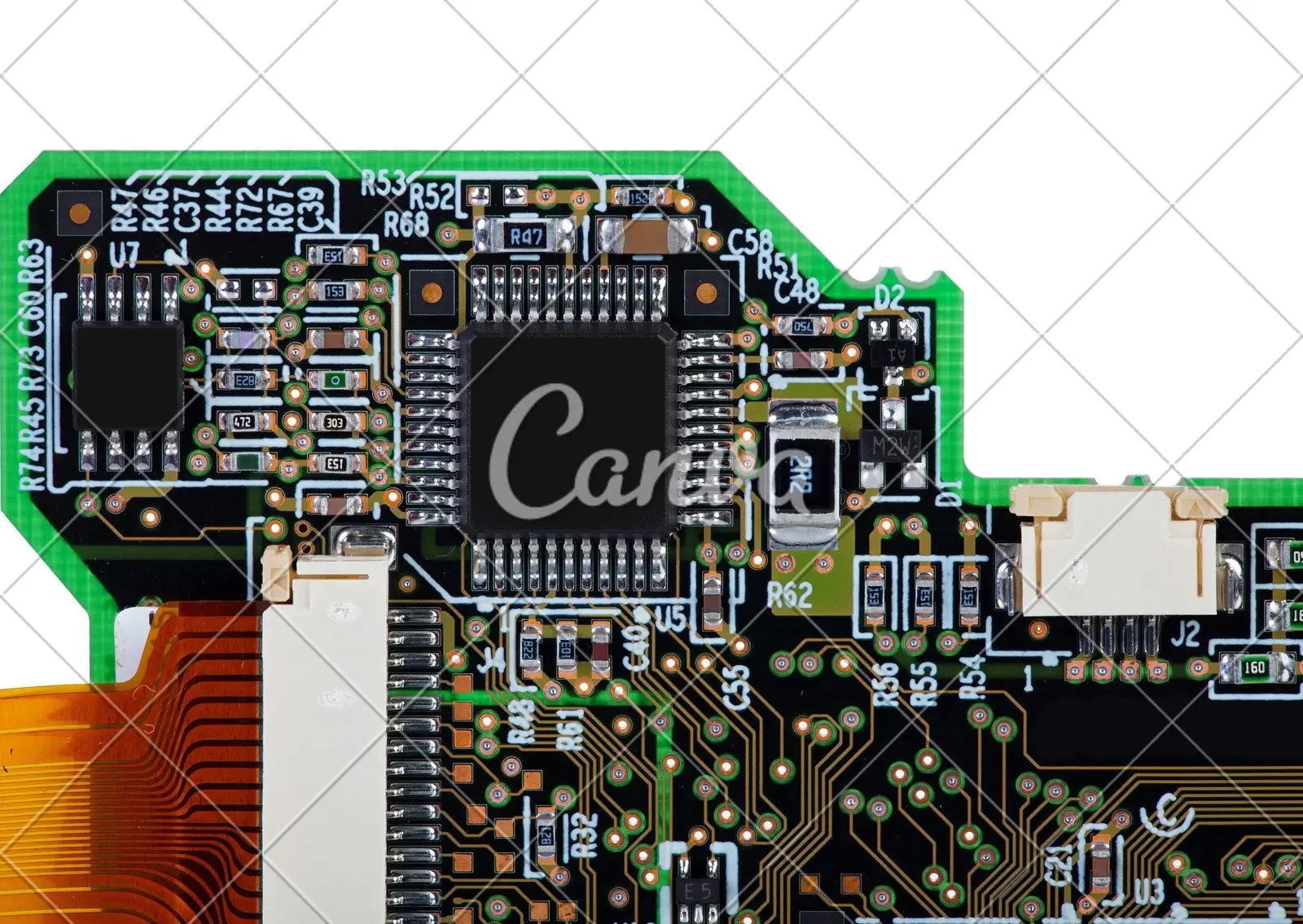
In daily life and work, it is often necessary to use a variety of electronIC and mechanical equipment. They have long been inseparable from daily life and become necessities of daily life. Such as computers, mobile phones, etc. The key component of those devices is PCB. PCB is also calLED circuit board, and the processing of circuit board is called pcba. PCBA must be designed and processed before PCB production and processing. So, what are the main methods of PCBa proofing?

1. Subtraction. This kind of method mainly uses chEMIcals to remove the unnecessary parts on the blank circuit board, and the remaining parts are the necessary circuits. The pcba design and processing mainly uses screen printing or photosensitive plates and engraving for processing, and the unnecessary parts are removed.
2. Addition method. This method is to expose the necessary places through the combination of ultraviolet ray and photoresist, then thicken the certificate line by electroplating, then coat the photoresist or metal thin tin, and finally remove the photoresist and the copper foil layer under the cover.
3. Lamination method. This kind of method is the most common method of PCBA Design and processing, and also the main method of making multilayer printed circuit board. It is to realize the fabrication of multilayer printed circuit boards by continuously repeating the process of lamination through processing from the inner layer to the outer layer, and then using the subtraction or addition method. The most critical process is the layer adding method, which adds the printed circuit board layer by layer for repeated processing.
Pcba proofing refers to the whole process of loading empty PCB boards through SMT and then through DIP plug-ins, which is calLED PCBa proofing. It is the customer's behavior to perform the SMT patch test again because of the need of new products. Nowadays, PCBA processing technology is widely used in daily life, mainly in the field of science and technology.
Although PCBA processing technology is widely used in our daily life, many people do not know what should be prepared when doing this work. Through research, it is found that the following documents need to be prepared for pcba proofing:
First, prepare a complete and accurate bill of materials. Then provide the Gerber file of the template. As far as possible, provide the product location number screen printing drawing and patch coordinate file, and finally provide the printed circuit board file.
In addition to the documents that need to be prepared mentioned above, there are also some matters that need to be noted during proofing. Because of these precautions, the whole work will be more efficient and the quality of products will be better. In the process of pcba processing, the following points should be noted:
Secondly, in order to use redundant ingredients in the manufacturing process, when preparing materials for surface mounting processing, several single plates and double plates should be prepared. Other low value materials should also be prepared more. However, large originals and chips do not require much preparation.
This paper introduces that pcba must be designed and processed before pcb production and processing


抖音二維碼

Q Q二維碼

微信二維碼
點擊
然后
聯(lián)系
然后
聯(lián)系
電話熱線
13410863085Q Q

微信

- 郵箱