鑫景福致力于滿足“快速服務(wù),零缺陷,輔助研發(fā)”PCBA訂購單需求。


PCBA加工
Summary of key points for manual assembly of the latest PCBA SMT electronIC products in 2022
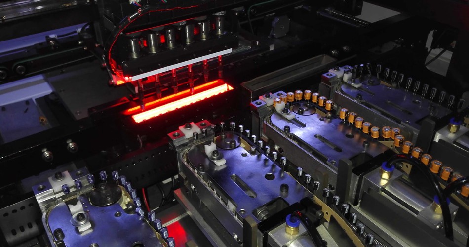
1. SMT (Surface Mount Technology) is a new generation of electronic mounting technology, which compresses the traditional electronIC components into devices with a volume of only one tenth of that of the traditional electronic components, thus realizing the high-density, highly reliable, miniaturized, low-cost and automatic production of electronic products.
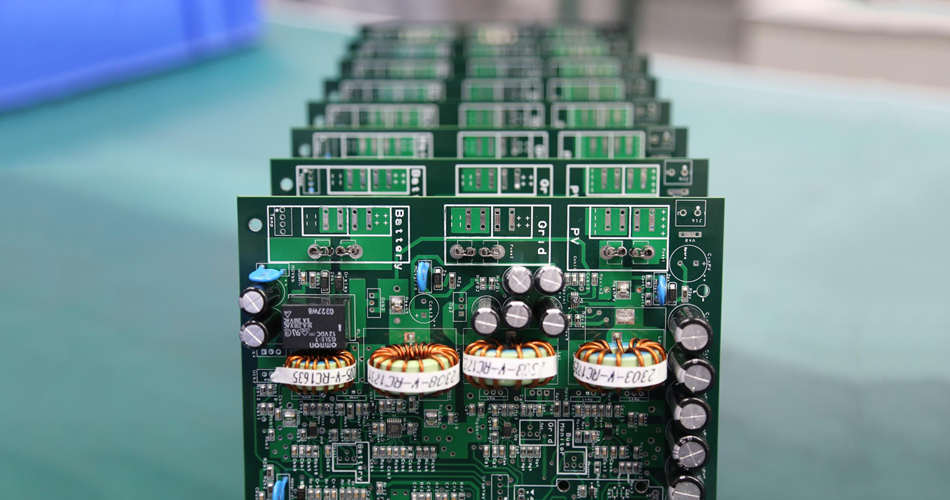
2. surface mounted components are mainly divided into chip passive components and active components. Their main characteristics are: miniaturization, no lead (flat or short lead, suitable for surface assembly on PCB.
3. The packaging form of surface mounted components directly affects the efficiency of assembly production, so it must be optimized according to the type and number of feeder of the mounting machine. There are four main packaging forms of surface mounted components, namely, tape weaving, tube packaging, pallet packaging and bulk packaging.
4. Solder is a fusible metal, which can form an alloy on the surface of the base metal and be connected with the base metal as a whole. It is not only used for mechanical connection, but also for electrical connection. In welding, it is customary to call the welding with the welding temperature lower than 450 ℃ soft soldering, and the solder used is also calLED soft solder. The welding temperature of electronic circuits is usually between 180 ℃ and 300 ℃. The main components of the solder used are tin and lead, so it is also called tin lead solder.
5. Solder paste is a mixture of solder powder and paste flux with soldering function. Generally, alloy solder powder accounts for 85%~90% of the total weight and 50% of the volume
6. Patch adhesive is also called adhesive. In the hybrid assembly, the surface mounted components are temporarily fixed on the PCB pad graphics, so that the subsequent wave soldering and other process operations can be carried out smoothly; In the case of double-sided surface assembly, assist in fixing the surface assembly components to prevent the surface assembly components from falling down in case of vibration during the turnover plate and process operation. Therefore, before assembling components on the mounting surface, it is necessary to set the pad position on the PCB and apply the patch adhesive.
7. There are two most common types of manual welding: contact welding and heated gas welding.
8. Heating control is a key factor in the desoldering process. The solder must be completely melted to avoid damaging the bonding pad when removing components.
9. The contents of desoldering design include: according to the type, size and packaging material of the device to be disassembled, the temperature range and air volume of the top and bottom heating are basically determined by using the standard database parameters provided by the repair device, and the appropriate hot air nozzle and vacuum nozzle are selected; According to the scope of desoldering operation, remove the surrounding components that affect the operation or apply necessary heat resistance measures to determine the heating time, etc.
10. After the ball grid array package is removed, the solder ball needs to be reformed, which is also known as ball planting. When BGA packaged devices are removed from PCB, some solder balls will always remain on the device and others will remain on the pad. Solder balls left on the pad are usually like solder icicles. If such devices are required to be reinstalled on the PCB, it is required to conduct all solder ball reforming and PCB pad cleaning preparation.
11. The repair process of BGA packaging devices can be divided into four steps:
① It is used to clean the residual solder balls or soldering tin on the bonding pad on BGA and the surface of PCB bonding pad, and to sort out the original solder ball pads to keep them flat. The flux and tin absorbing tape with the same chEMIcal composition as those in the original assembly process shall be used as much as possible during processing, which will reduce the possibility of deposition of residues on the ball grid array surface and the lower side of SMAll packaging devices such as CSP or flip chip;
② It is to evenly apply the prepared flux to the bonding pad;
③ It is to manually transplant the prepared solder ball particles corresponding to the diameter of the original device solder ball to the corresponding pad;
④ According to the temperature requirements of the solder ball and flux, the BGA of the completed planting ball is placed in a suitable temperature atmOSPhere to "solidify" so that the solder ball and the pad can be closely and reliably connected.
The above is a summary of the key points of manual assembly of the latest PCBA SMT electronic products in 2022 explained by the circuit board manufacturer.
Packaging in PCBA processing
10-26,2022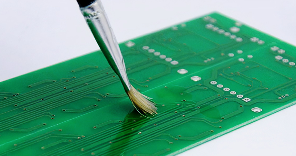


抖音二維碼

Q Q二維碼

微信二維碼
點擊
然后
聯(lián)系
然后
聯(lián)系
電話熱線
13410863085Q Q

微信

- 郵箱