鑫景福致力于滿足“快速服務,零缺陷,輔助研發”PCBA訂購單需求。


PCBA方案設計
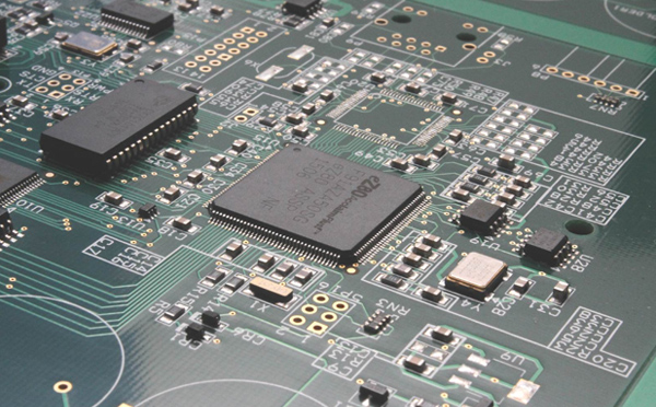
Requirements of SMT process on component layout
The Layout of components shall be designed according to the characteristICs and requirements of SMT electronic processing equipment and process. Different processes, such as reflow soldering and wave soldering, have different layouts of components. When reflow soldering on both sides, there are different requirements for the layout of side A and side B; Selective wave soldering and traditional wave soldering also have different requirements.
The basic requirements of SMT process for component layout design are as follows:
The distribution of components on the printed circuit board should be as uniform as possible. The thermal capacity of high-quality components is large when reflow soldering, and excessive concentration is likely to cause low local temperature and lead to faulty soldering; At the same time, the uniform layout is also conducive to the balance of the center of gravity. In the vibration impact test, it is not easy for components, metallized holes and pads to be damaged.
The arrangement direction of components on the printed circuit board. SIMilar components shall be arranged in the same direction as far as possible, and the feature direction shall be consistent, so as to facilitate the mounting, welding and testing of components. For example, the positive pole of the electrolytic capacitor, the positive pole of the diode, the single pin end of the triode, and the first pin of the integrated circuit shall be arranged in the same direction as far as possible. All component numbers shall be printed in the same direction.
The size that SMD repair equipment heater can operate shall be reserved around large components.
The heating components shall be as far away from other components as possible, and generally placed at the corner and ventilation position in the case. The heating components shall be supported by other leads or other supports (such as heat sink) to keep a certain distance between the heating components and the surface of the printed circuit board, with a minimum distance of 2mm. The heating components connect the heating components body with the printed circuit board in the multilayer board. The metal bonding pad is made in the design, and the soldering tin is used in the processing, so that the heat is distributed through the printed circuit board.
Temperature sensitive components shall be far away from heating components. For example, triodes, integrated circuits, electrolytic capacitors and some molded case components should be as far away from bridge stacks, high-power components, radiators and high-power resistors as possible.
The layout of components and parts that need to be adjusted or frequently replaced, such as potentiometers, adjustable inductance coils, variable capacitor microswitches, safety tubes, keys, pluggers and other components, shall consider the structural requirements of the whole machine and place them in positions that are convenient for adjustment and replacement. If it is adjusted in the machine, it should be placed on the printed circuit board where it is easy to adjust; If it is adjusted outside the machine, its position shall be consistent with the position of the adjustment knob on the chassis panel to prevent conflict between three-dimensional space and two-dimensional space. For example, the panel opening of the button switch should match the position of the switch space on the printed circuit board.
Fixing holes shall be set near the terminal blocks, plug and pull pieces, the center of long string terminals and the parts frequently under force, and corresponding space shall be reserved around the fixing holes to prevent deformation due to thermal expansion. For example, the thermal expansion of the long string terminal is more serious than that of the printed circuit board, and it is easy to be warped during wave soldering.
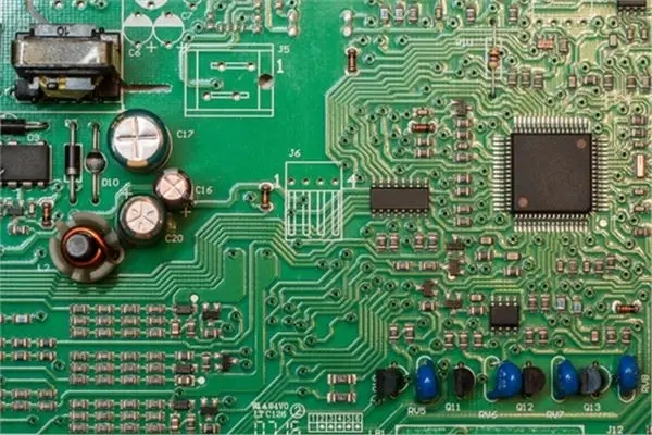
Some components and parts (such as transformers, electrolytic capacitors, varistors, bridge stacks, radiators, etc.) that require secondary processing due to large volume (surface) tolerance and low accuracy shall be provided with a certain margin on the basis of the original settings.
It is recommended that the increased margin of electrolytic capacitors, varistors, bridge stacks, polyester capacitors, etc. should not be less than 1mm, and that of transformers, radiators, and resistors over 5W (including 5W) should not be less than 3mm
The electrolytic capacitor shall not touch the heating components, such as high-power resistance thermistor, transformer, radiator, etc. The minimum spacing between electrolytic capacitor and radiator is 10mm, and that between other components and radiator is 20mm.
The stress sensitive components shall not be placed at the corners and edges of the printed circuit board or near the connectors, mounting holes, slots, cuts, notches and corners of the panel. The above positions are high stress areas of the printed circuit board, which are likely to cause cracks or cracks in solder joints and components.
The layout of components shall meet the process requirements and spacing requirements of reflow soldering and wave soldering. Reduce shadow effect during wave soldering.
The positioning hole of printed circuit board and the position needed for fixing bracket shall be reserved.
In the design of large-area printed circuit board with an area of more than 500cm2, in order to prevent the printed circuit board from bending when passing through the tin furnace, a 5~10mm wide gap should be left in the middle of the printed circuit board, without placing components (wiring is allowed), so as to add a strip to prevent the printed circuit board from bending when passing through the tin furnace.
Layout direction of components for reflow soldering process.
① The placement direction of components shall consider the direction of PCB entering the reflow soldering furnace.
② In order to make the welding ends on both sides of the two end piece components and the pins on both sides of the SMD components heated synchronously, and to reduce the welding defects such as standing stone, displacement, and the welding end leaving the bonding pad caused by the failure of the welding ends on both sides of the components to be heated synchronously, it is required that the long axis of the two end piece elements on the printed circuit board should be perpendicular to the direction of the conveyor belt of the reflow soldering furnace.
③ The long axis of SMD components shall be parallel to the transmission direction of reflow soldering furnace, and the long axis of chip components at two ends shall be perpendicular to the long axis of SMD components.
④ A good component layout design should not only consider the uniformity of thermal capacity, but also consider the layout direction and order of components,
⑤ For large size printed circuit board, in order to keep the temperature on both sides of the printed circuit board as consistent as possible, the long side of the printed circuit board should be parallel to the direction of the conveyor belt of the reflow soldering furnace. Therefore, when the size of printed circuit board is greater than 200mm, the requirements are as follows:
a) The long axis of the chip components at the two ends is perpendicular to the long side of the printed circuit board.
b) The long axis of SMD components is parallel to the long side of the printed circuit board.
c) The components on both sides of the printed circuit board assembLED on both sides have the same orientation.
d) The arrangement direction of components on the printed circuit board. Similar components shall be arranged in the same direction as far as possible, and the feature direction shall be consistent, so as to facilitate the mounting, welding and testing of components. For example, the positive pole of the electrolytic capacitor, the positive pole of the diode, the single pin end of the triode, and the first pin of the integrated circuit shall be arranged in the same direction as far as possible.
In order to prevent short circuit between layers caused by touching the printed wire during PCB processing, the conductive pattern at the inner and outer edges should be more than 1.25 mm from the PCB edge. When a grounding wire has been laid on the edge of the outer layer of PCB, the grounding wire can occupy the edge position. For PCB board positions that have been occupied due to structural requirements, no components and printed wires can be laid, and no through-hole is allowed in the bottom pad area of SMD/SMC, so as to avoid solder splitting after being heated and remelted in wave soldering after reflow soldering.
Installation distance of components: the minimum installation distance of components must meet the requirements of manufacturability, testability and maintainability of SMT assembly.
PCB design and anti deformation design
10-27,2022


抖音二維碼

Q Q二維碼

微信二維碼
點擊
然后
聯系
然后
聯系
電話熱線
13410863085Q Q

微信

- 郵箱