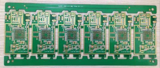
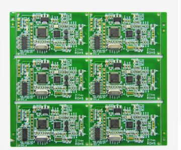
鑫景福致力于滿足“快速服務,零缺陷,輔助研發”PCBA訂購單需求。


PCBA方案設計
The multi-layer board and the double-layer board are SIMilar in design and even easier to route.
If you have experience in the design of double-layer boards, it is not diffICult to have multiple layers.
First of all, it is necessary to divide the layered structure, with the substrate as the center, symmetrically distributed to both sides, and the adjacent signal layers are separated by electrical ground layers. It is the most convenient to design.
Laminated structure (4 layers, 6 layers, 8 layers, 16 layers):
For the transmission line, the microstrip line model is used for the top and bottom layers, and the stripline model is used for the internal signal layer. The signal layers on both sides of the 6-layer/10-layer/14-layer/18-layer substrate are best simulated by software, which is more troublesome.
There are signal layers on both sides of the substrate such as 6-layer/10-layer/14-layer/18-layer, and there is no electrical isolation. It is necessary to pay attention to the vertical wiring of adjacent layers and avoid AC loops.
If there are other power sources, give priority to thick lines on the signal layer, and try not to divide the electrical ground layer
Multilayer circuit board design principles
Most PCB engineers, they often draw computer motherboards, are very proficient with excellent tools such as Allegro, but, unfortunately, they rarely know how to perform impedance control and how to use tools for signal integrity analysis. How to use IBIS Model. I think a real PCB expert should still be a signal integrity expert, not just on the basis of connections and vias. It is easy to fabricate a board, but difficult to fabricate a good one.

After the number of power supply, ground layers and signal layers is determined, the relative arrangement between them is a topic that every PCB engineer cannot avoid;
General Principles of Layer Arrangement
The ground plane is below the component surface (the second layer), providing the device shielding layer and the reference plane for the top layer wiring;
All signal layers are as adjacent to the ground plane as possible;
The situation where the two signal layers are directly adjacent should be avoided as much as possible;
The main power supply should be adjacent to its corresponding as far as possible;
Take into account the symmetry of the laminated structure.
For the layer layout of the motherboard, it is difficult for the existing motherboard to control parallel long-distance wiring. For the board-level operating frequency above 50MHZ (the case below 50MHZ can be referred to and appropriately relaxed), the recommended layout principles:
The component surface and welding surface are a complete ground plane (shielding);
No adjacent parallel wiring layers;
All signal layers are as adjacent to the ground plane as possible;
Critical signals are adjacent to the formation and do not cross partitions.
Note: When setting the layers of the specific PCB, the above principles should be flexibly grasped. On the basis of understanding the above principles, according to the actual needs of the single board,
Commonly used stacking scheMES
The following uses an example of a 4-layer board to illustrate how to optimize the arrangement and combination of various laminated structures.
4 layer stacking scheme (from top to bottom)
Siganl_1 (Top), GND (Inner_1), POWER (Inner_2), Siganl_2 (Bottom).
Siganl_1 (Top), POWER (Inner_1), GND (Inner_2), Siganl_2 (Bottom).
POWER (Top), Siganl_1 (Inner_1), GND (Inner_2), Siganl_2 (Bottom).
Obviously, option 3 lacks effective coupling between the power supply layer and the ground layer and should not be used.

So how should option 1 and option 2 be chosen? Under normal circumstances, designers will choose scheme 1 as the structure of the 4-layer board. The reason for the choice is not that scheme 2 cannot be used, but that general PCB boards only place components on the top layer, so scheme 1 is more appropriate. However, when components need to be placed on both the top and bottom layers, and the dielectric thickness between the internal power supply layer and the ground layer is large and the coupling is poor, it is necessary to consider which layer has fewer signal lines. For scheme 1, there are fewer signal lines on the bottom layer, and a large-area copper film can be used to couple with the POWER layer; on the contrary, if the components are mainly arranged on the bottom layer, scheme 2 should be used to make the board.
If the power layer and the ground layer are already coupLED, considering the requirements of symmetry, scheme 1 is generally used.
6-layer stacking scheme
Scheme 1: Siganl_1 (Top), GND (Inner_1), Siganl_2 (Inner_2), Siganl_3 (Inner_3), POWER (Inner_4), Siganl_4 (Bottom). Scheme 1 uses 4 layers of signal layers and 2 layers of internal power/ground layers, and has more signal layers, which is conducive to the wiring work between components, but the defects of this scheme are also more obvious, which are manifested in the following two aspects.
The power and ground planes are far apart and not fully coupled.
The signal layers Siganl_2 (Inner_2) and Siganl_3 (Inner_3) are directly adjacent to each other, so the signal isolation is not good and crosstalk is prone to occur.
Scheme 2: Siganl_1 (Top), Siganl_2 (Inner_1), POWER (Inner_2), GND (Inner_3), Siganl_3 (Inner_4), Siganl_4 (Bottom). Compared with scheme 1, scheme 2 has sufficient coupling between the power supply layer and the ground layer, which has certain advantages over scheme 1, but the Siganl_1 (Top) and Siganl_2 (Inner_1) and Siganl_3 (Inner_4) and Siganl_4 (Bottom) signal layers are directly Adjacent, the signal isolation is not good, and the problem of easy crosstalk has not been solved.
Scheme 3: Siganl_1 (Top), GND (Inner_1), Siganl_2 (Inner_2), POWER (Inner_3), GND (Inner_4), Siganl_3 (Bottom). Compared with scheme 1 and scheme 2, scheme 3 reduces one signal layer and adds an internal electrical layer. Although the layers available for wiring are reduced, this scheme solves the common defects of scheme 1 and scheme 2.

The power and ground planes are tightly coupled.
Each signal layer is directly adjacent to the inner electrical layer, and is effectively isolated from other signal layers, so crosstalk is not easy to occur.
Siganl_2 (Inner_2) is adjacent to the two inner electrical layers GND (Inner_1) and POWER (Inner_3), which can be used to transmit high-speed signals. The two inner electrical layers can effectively shield the external interference to the Siganl_2 (Inner_2) layer and the interference of Siganl_2 (Inner_2) to the outside world.
In all aspects, scheme 3 is obviously the most optimized one. At the same time, scheme 3 is also a commonly used laminated structure for 6-layer boards.
Through the analysis of the above two examples, I believe that readers have a certain understanding of the casCADing structure, but in some cases, a certain solution cannot meet all the requirements, which requires consideration of the priority of various design principles. Unfortunately, since the layer design of the multilayer board is closely related to the characteristics of the actual circuit, the anti-interference performance and design focus of different circuits are different, so in fact, these principles do not have a definite priority for reference. But it can be determined that the design principle: the internal power supply layer and the ground layer should be tightly coupled, which needs to be satisfied first in the design. In addition, if high-speed signals need to be transmitted in the circuit, then design principle 3 (the high-speed signal transmission layer in the circuit should be is a signal intermediate layer, and is sandwiched between two internal electrical layers) must be satisfied.


抖音二維碼

Q Q二維碼

微信二維碼
點擊
然后
聯系
然后
聯系
電話熱線
13410863085Q Q

微信

- 郵箱