鑫景福致力于滿足“快速服務,零缺陷,輔助研發”PCBA訂購單需求。


PCBA方案設計
No.1 Data input stage
Whether the data received in the process are complete (including schematIC diagram, *. brd file, bill of materials, PCB design description, PCB design or change requirements, standardization requirements description, process design description and other documents).
Verify that the PCB templateis up to date.
Whether the layout of clock devices is reasonable.
Confirm that the position of the positioner of the template is correct.
Whether the description, PCB design or change requirements and standardization are clear.
Confirm that the prohibited components and wiring areas on the outline drawing have been reflected on the PCB template.
Compare the outline drawing to confirm that the dimensions and tolerances MARKed on the PCB are correct, and the definition of metallized holes and nonmetallic holes is accurate.
After confirming that the PCB template is correct, it is better to lock the structure file to avoid misoperation of the moved position.
No.2 Post layout inspection stage
1. PCB component inspection
Confirm whether the package of all devices is consistent with the company's unified library, and whether the package library has been updated (check the running results with the viewlog). If not, you must update Symbols.
Motherboard and daughter board, single board and backplane, confirm that the signals and positions are corresponding, the connector direction and silk screen identification are correct, the daughter board has anti misplug measures, and the components on the daughter board and motherboard should not interfere.
Whether the components are placed 100%.
Open the place ground of the TOP and BOTTOM layers of the device, and check whether the DRC caused by overlap is allowed.
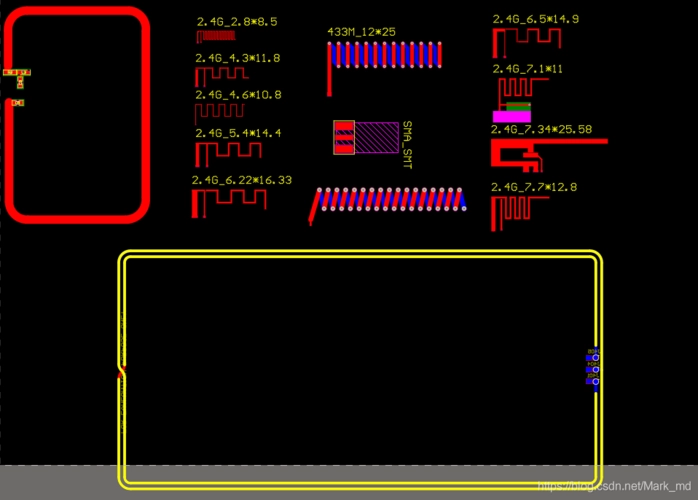
Whether Mark points are sufficient and necessary.
Heavy components should be placed close to PCB support points or edges to reduce PCB warpage.
Confirm whether the package of all devices is consistent with the company's unified library, and whether the package library has been updated (check the running results with the viewlog). If not, you must update Symbols.
Motherboard and daughter board, single board and backplane, confirm that the signals and positions are corresponding, the connector direction and silk screen identification are correct, the daughter board has anti misplug measures, and the components on the daughter board and motherboard should not interfere.
Whether the components are placed 100%.
Open the place ground of the TOP and BOTTOM layers of the device, and check whether the DRC caused by overlap is allowed.
Whether Mark points are sufficient and necessary.
Heavy components should be placed close to PCB support points or edges to reduce PCB warpage.
It is better to lock the devices related to the structure after they are arranged to prevent maloperation of moving position.
Within the range of 5mm around the crimping socket, no element with a height higher than the crimping socket is allowed on the front, and no element or solder joint is allowed on the back.
Confirm whether the device layout meets the process requirements (focus on BGA, PLCC, SMD socket).
Special attention shall be paid to components with metal shells not to collide with other components, and enough space shall be reserved.
The components related to the interface shall be placed as close to the interface as possible, and the backplane bus driver shall be placed as close to the backplane connector as possible.
Whether the chip device on the wave soldering surface has been converted to wave soldering package.
Whether there are more than 50 manual welding points.
Horizontal installation should be considered for axial insertion of higher components on PCB. Leave room for lying. And consider the fixing method, such as the fixed pad of the crystal oscillator.
For components requiring heat sink, make sure there is enough space between them and other components, and pay attention to the height of main components within the range of heat sink.
2. Functional check
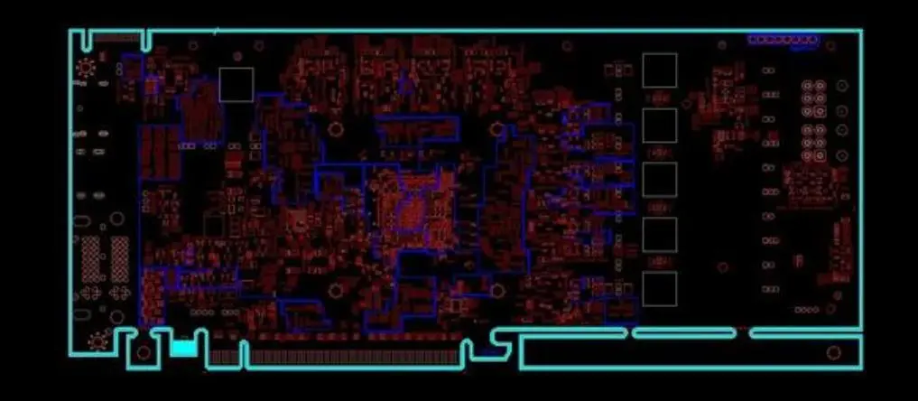
Whether the digital circuit and analog circuit components of the digital analog mixing board have been separated in layout, and whether the signal flow is reasonable.
A/D converters are placed across analog digital partitions.
Whether the layout of clock devices is reasonable.
Whether the layout of high-speed signal devices is reasonable.
Whether the termination devices have been properly placed (the source matching serial resistance should be placed at the driving end of the signal; the intermediate matching serial resistance should be placed at the middle position; the terminal matching serial resistance should be placed at the receiving end of the signal)
The signal line takes the plane of different levels as the reference plane. When crossing the plane division area, whether the connection capacitance between the reference planes is close to the signal routing area.
Whether the layout of the protection circuit is reasonable and conducive to division. Whether the fuse of the board power supply is placed near the connector and there are no circuit components in front of it.
Confirm that strong signal and weak signal (power difference of 30dB) circuits are laid separately.
Whether the number and position of decoupling capacitors of IC devices are reasonable.
Whether the components that may affect the EMC experiment are placed according to the design guide or reference to successful experience. For example, the reset circuit of the panel should be slightly close to the reset button.
3. Fever
Thermal sensitive PCB components (including liquid dielectric capacitors and crystal oscillators) shall be kept away from high-power components, radiators and other heat sources as far as possible.
Whether the layout meets the thermal design requirements and the heat dissipation channel (according to the PCB process design document).


抖音二維碼

Q Q二維碼

微信二維碼
點擊
然后
聯系
然后
聯系
電話熱線
13410863085Q Q

微信

- 郵箱