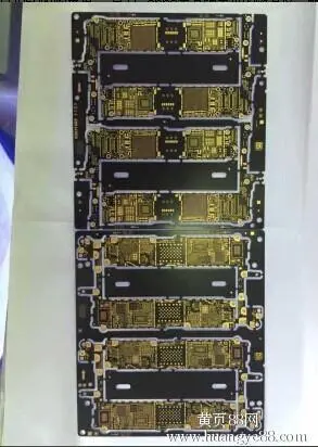
鑫景福致力于滿足“快速服務(wù),零缺陷,輔助研發(fā)”P(pán)CBA訂購(gòu)單需求。


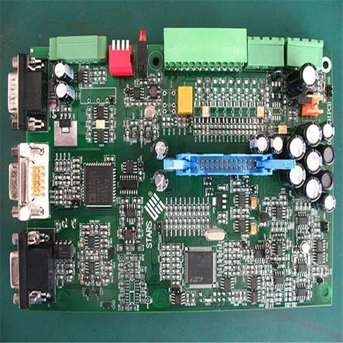
PCBA方案設(shè)計(jì)
In the IC application design, after the schematIC design of the project is completed, PCB layout design is required. Is a crucial link. The quality of the design result directly affects the whole design function. Therefore, a reasonable and efficient PCB layout is a crucial step in the success of chip circuit design and debugging. This time we will briefly talk about the design points of PCB Layout.
Key Points of PCB layout design
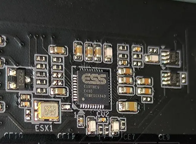
component packaging selection
resistance selection: withstand voltage, maximum power consumption and temperature of the selected resistance shall not exceed the range of use.
Capacitor selection: the withstand voltage and maximum effective current of the selected capacitor shall also be considered.
Inductance selection: the effective value current and peak current of the selected inductor must be greater than the current flowing in the actual circuit.
Common interference in circuit design
Crosstalk: when the distance between parallel lines of the design line is too long, mutual capacitance and mutual inductance between conductors will couple energy to adjacent transmission lines. The crosstalk impact can be reduced by:
1. Add safe routing
2. In practice, try to make adjacent routes perpendicular to each other
3. Increase the distance between parallel lines for each distance
Reflection: The impedance of transmission line does not match due to too many corners and branches of PCB wiring. It can be improved by reducing corners and branch lines on the line or avoiding right angle routing and branch line reinforcement.
Determine the grounding mode
Single point grounding (applicable to low-frequency circuits): all circuit grounding wires are connected to the same point of the common ground wire, which is SIMple to connect and reduces mutual interference between ground wire loops.
Multipoint grounding (applicable to multilayer circuit/high-frequency circuit): all parts of the system are grounded nearby to provide low grounding impedance.
Increase filter and bypass capacitance
To ensure the stability of input/output voltage, increase input/output capacitance.
A bypass capacitor is added between the power supply and IC to ensure the stability of the input voltage and filter out high-frequency noise.
Impedance position design
Relatively speaking, the higher the impedance is, the easier it is to be interfered. The following is the PCB impedance position design of a synchronous buck chip.
PCB Layout Design Skills
Power/ground handling
Even though the wiring in the whole PCB board is well completed, the interference caused by improper consideration of power supply and ground wire will degrade the product performance When wiring, the width of power supply and ground wire shall be widened as much as possible. It is better that the ground wire is wider than the power wire. Their relationship is: ground wire>power wire>signal wire.
PCB of digital circuit can be used to form a loop with wide ground wire, that is, to form a ground grid (this method cannot be used for analog circuit). Use a large area of copper layer as ground wire, and connect all unused parts on the PCB with the ground as ground wire. Or it can be made into multilayer boards, with one layer for power supply and one layer for ground wire.
Common Ground Processing of Digital and Analog Circuits
Common ground processing of digital circuit and analog circuit: when digital circuit and analog circuit exist together, the mutual interference between them should be considered for wiring, especially the noise interference on the ground wire.
The frequency of digital circuit is high, and the sensitivity of analog circuit is strong. For signal lines, high-frequency signal lines should be as far away from sensitive analog circuit devices as possible,
As for the ground wire, the external connection boundary of the entire PCB has only one port, so it is necessary to deal with the problem of digital and analog common ground inside the PCB. In fact, the digital ground and analog ground inside the board are not connected to each other, but there is a short circuit between the digital ground and analog ground at the ports (such as plugs) where the PCB is connected to the outside. Please note that there is only one connection point.
PCB signal line distribution layer
PCB signal lines are laid on the power (ground,
To solve this contradiction, PCB wiring on the electrical (ground) layer can be considered. The power layer should be considered first, and then the stratum. Because it is better to preserve the integrity of the stratum.


抖音二維碼

Q Q二維碼

微信二維碼
點(diǎn)擊
然后
聯(lián)系
然后
聯(lián)系
電話熱線
13410863085Q Q

微信

- 郵箱