鑫景福致力于滿足“快速服務,零缺陷,輔助研發”PCBA訂購單需求。


PCBA方案設計
Printed circuit board (PCB) routing plays a key role in high-speed circuits, but it is often one of the last steps in the circuit design process. High speed PCB wiring has many problems, and a large number of literatures have been written on this topIC. This paper mainly discusses the wiring problem of high-speed circuit from the perspective of practice. The main purpose is to help new users pay attention to various problems that need to be considered when designing high-speed circuits. Another purpose is to provide a review material for
customers who have not touched PCB wiring for some time. Due to the limited layout, it is impossible to discuss all the problems in detail in this paper, but we will discuss the key parts that have the greatest effect on improving circuit performance, shortening design time and saving modification time.
Although this paper mainly focuses on PCB circuits related to high-speed operational amplifiers, the problems and methods discussed here are generally applicable to the wiring of most other high-speed analog circuits. When the operational amplifier works in a very high RF band, the performance of the circuit largely depends on PCB wiring. High performance circuit design that looks good on the "drawing" can only achieve ordinary performance if it is affected by careless wiring. Anticipating and paying attention to important details throughout the wiring process will help ensure the expected circuit performance.
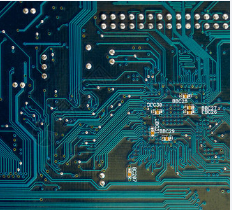
PCB wiring
schematic diagram
Although good schematics cannot guarantee good wiring, good wiring starts with good schematics. When drawing the schematic diagram, you must think carefully and consider the signal flow direction of the whole circuit. If there is a normal and stable signal flow from left to right in the schematic diagram, then there should be the same good signal flow on the PCB. Give as much useful information as possible on the schematic diagram. Because sometiMES the circuit design engineer is absent, customers will ask us to help solve the circuit problems. Designers, technicians and engineers engaged in this work will be very grateful, including us.
In addition to the common reference identifier, power consumption and error tolerance, what information should be given in the schematic diagram? Here are some suggestions to turn a common schematic into a first-class schematic. Add waveform, mechanical information about housing, length of printed wire and blank area; Indicate which components need to be placed on the PCB; Give adjustment information, element value range, heat dissipation information, control impedance printed wire, notes, and brief circuit action description
position
Just as in a PCB, position determines everything. It is very important to place a circuit on a PCB, to install its specific circuit components, and to identify other adjacent circuits
Usually, the positions of input, output and power supply are predetermined, but the circuits between them need to "give play to their creativity". This is why paying attention to the details of cabling can pay off handsomely. Start from the position of key components, and consider according to the specific circuit and the entire PCB. Specifying the location of key components and the path of signals from the beginning helps to ensure that the design achieves the desired work objectives. Getting the right design once can reduce cost and pressure - and shorten the development cycle.
bypass source
It is a very important aspect in the process to bypass the power supply at the power supply end of the amplifier in order to reduce noise - including high-speed operational amplifiers or other high-speed circuits. There are two common configuration methods for bypass high-speed operational amplifiers.
Power supply terminal grounding: This method is the most effective in most cases. Multiple parallel capacitors are used to directly ground the power supply pin of the operational amplifier. In general, two shunt capacitors are sufficient - but adding shunt capacitors may benefit some circuits.
Shunting capacitors with different capacitance values helps ensure that the power supply pin can only see very low AC impedance in a very wide frequency band. This is especially important at the attenuation frequency of the power supply rejection ratio (PSR) of the operational amplifier. This capacitor helps compensate for the reduced PSR of the amplifier. Maintaining a low impedance ground path over many octave ranges will help ensure that harmful noise does not enter the op amp. Figure 1 shows the advantages of using multiple parallel capacitors. In the low frequency band, large capacitors provide a low impedance grounding path. But once the frequency reaches its own resonant frequency, the capacitance of the capacitor will be weakened, and gradually become inductive. This is why it is important to use multiple capacitors: when the frequency response of one capacitor starts to decline, the frequency response of the other capacitor starts to function, so it can maintain a very low AC impedance in many octave ranges.
Ground plane
In fact, the content to be discussed is far more than that mentioned in this article, but we will highlight some key features and encourage readers to further explore this topic. At the end of this paper, relevant references are listed.
The ground plane acts as a common reference voltage, providing shielding, cooling and reducing parasitic inductance (but it also increases parasitic capacitance). Although there are many advantages to using a ground plane, you must be careful when implementing it, because it has some limitations on what you can and cannot do.
Ideally, the PCB should have a layer dedicated to the ground plane. This will produce the best results when the entire plane is not damaged. Never use the area of the grounding plane in this special layer to connect other signals. Since the grounding plane can eliminate the magnetic field between the conductor and the grounding plane, the inductance of the printed wire can be reduced. If a certain area of the grounding plane is damaged, unexpected parasitic inductance will be introduced to the printed PCB wires above or below the grounding plane.
Because the ground plane usually has a large surface area and cross-sectional area, the resistance of the ground plane is kept to a minimum. In the low frequency band, the current will choose the path with the least resistance, but in the high frequency band, the current will choose the path with the least resistance.
However, there are exceptions. Sometimes a SMAll ground plane is better. If the grounding plane is removed from the input or output pad, the high-speed operational amplifier will work better. Because the parasitic capacitance introduced in the grounding plane of the input terminal increases the input capacitance of the operational amplifier and reduces the phase margin, it causes instability. As we saw in the discussion in the Parasitic Effects section, the capacitance of 1 pF at the input of the operational amplifier can cause sharp pulses. Capacitive loads at the output -- including parasitic capacitive loads -- create poles in the feedback loop. This reduces the phase margin and causes the circuit to become unstable.
If possible, analog and digital circuits - including their respective ground and ground planes - should be separated. The fast rising edge will cause current burrs to flow into the grounding plane. The noise caused by these fast current burrs will damage the SIMulation performance. Analog ground and digital ground (and power supply) shall be connected to a common ground point to reduce circulating digital and analog ground current and noise.
High level PCB wiring is very important for successful operational amplifier circuit design, especially for high-speed circuits. A good schematic diagram is the basis of good wiring; The close cooperation between circuit design engineers and wiring design engineers is fundamental, especially with respect to the location of devices and wiring. The problems to be considered include bypass power supply, reduction of parasitic effect, use of grounding plane, impact of operational amplifier packaging, and wiring and shielding methods.
1. In PCB design, capacitors such as bypass filter at chip power supply should be as close to the device as possible, and the typical distance is less than 3MM.
2. The small ceramic bypass capacitor at the power supply of the operational amplifier chip can provide the choice of energy capacitance value for the high-frequency characteristics of the amplifier when the amplifier is in the input high-frequency signal. For example, a 400MHz amplifier may use 0.01uF and 1nF capacitors instalLED in parallel.
3. When we buy capacitors and other devices, we also need to pay attention to their self resonant oscillation frequency. Capacitance with a self resonant frequency above or below this frequency (400MHz) is useless.
4. When drawing a PCB, do not run other lines under the input/output signal pin of the amplifier and the feedback resistor, which can reduce the mutual influence of parasitic capacitance between different lines and make the amplifier more stable
5. High frequency performance of surface mount devices is good and small
6. The wiring of the circuit board shall be as short as possible while paying attention to its length and width to minimize parasitic effects
PCB Design of Four layer PCB Process
10-30,2022


抖音二維碼

Q Q二維碼

微信二維碼
點擊
然后
聯系
然后
聯系
電話熱線
13410863085Q Q

微信

- 郵箱