鑫景福致力于滿足“快速服務,零缺陷,輔助研發”PCBA訂購單需求。


PCBA方案設計
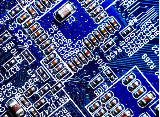
When making a PCB, if it is just an ordinary board, just do a good job of precise design of mechanICal dimensions. However, if high frequency signals, load lines or long lines are encountered, special treatment should be carried out for these lines. Otherwise, a series of signal interference problems, such as reflection and crosstalk between lines, may be caused. Therefore, when we are doing circuit design, especially high-speed PCB design, we must do a good job of emulating interference of line signal, and shielding measures are very necessary. Now let's talk about the PCB wiring and how to do the EMC design?
Suitable conductor width
When selecting the wire width, it is necessary to ensure its electrical performance and facilitate production, and it is usually determined by the minimum current it bears. In order to reduce the electromagnetic interference impact caused by transient current on PCB, it is necessary to control the line width in the design. Transient interference is generally caused by the inductance of the wire. Its inductance is proportional to the length of the wire and inversely proportional to the line width. As the signal line often has a large transient current, short and wide wires should be used. If the layout space allows, the herringbone MESh PCB layout structure should be used as far as possible.
. Key points of PCB component wiring
Component wiring design mainly considers several aspects: first, electrical performance; When wiring, we should try to put the devices closely connected with the wires together. The layout of high-speed lines should be as short as possible. Power devices and SMAll signal devices should be separated. The second is the placement position; Whether the design is beautiful and neat, and whether it is convenient for function test, later interface and connection. In high-speed systems, the transmission delay of grounding and interconnects is also the first design factor we need to consider. The transmission time of signal transmission lines has a great impact on the overall system speed of the circuit. If ordinary interconnects are used where high-speed lines are used, the delay time will increase and the system speed will be greatly reduced.
3. Wiring rules for high frequency PCB high-speed signals
Generally, the equal PCB wiring can reduce the inductance between wires, but in order to suppress the crosstalk of PCB circuit wires, we should try to avoid long distance equal wiring when designing the wiring; When designing printed PCB wires, sharp turns should be avoided, and curves with uniform and certain radians should be designed as far as possible; components with large current on the circuit shall be grounded separately as far as possible to avoid noise interference, and grounding shall be set between small signal or sensitive signal lines; Differential signal wiring design is adopted for high-speed signal, so that the two differential lines in the positive and negative pairs always keep the transmission lines coupLED, effectively reducing the electrical noise effect of the signal


抖音二維碼

Q Q二維碼

微信二維碼
點擊
然后
聯系
然后
聯系
電話熱線
13410863085Q Q

微信

- 郵箱