鑫景福致力于滿足“快速服務,零缺陷,輔助研發(fā)”PCBA訂購單需求。


PCBA方案設計
When talking about printed circuit boards, novICes often confuse "PCB schematic diagram" and "", but actually they refer to different things. Understanding the differences between them is the key to successful PCB manufacturing. Therefore, in order to enable beginners to do this better, this paper will decompose the key differences between PCB schematic and PCB design.
What is PCB
Before entering into the difference between schematic and design, what is PCB?
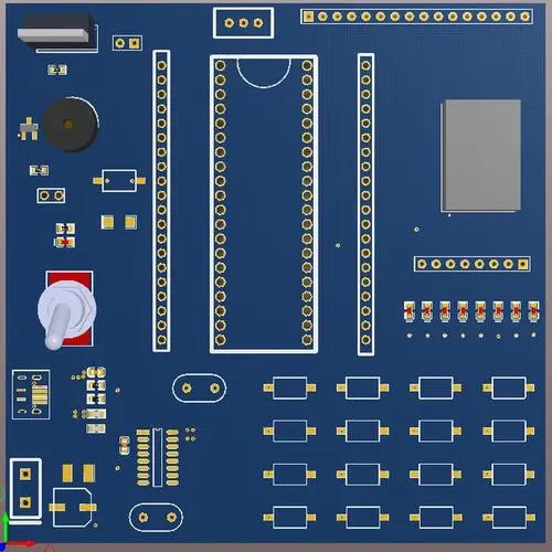
There are basically printed circuit boards in electronic equipment, also known as printed circuit boards. This green circuit board made of precious metal connects all electrical components of the equipment and enables them to operate normally. Without PCB, the electronic device will not work.
PCB schematic diagram and
PCB schematic diagram is a SIMple two-dimensional circuit design, showing the functions and connectivity between different components. The PCB design is a three-dimensional layout, which MARKs the position of components after ensuring the normal operation of the circuit.
Therefore, PCB schematic is the first part of PCB design. This is a graphical representation that uses agreed symbols to describe circuit connections, whether written or data. It also prompts the components to be used and how they are connected.
As the name implies, a PCB schematic is a plan and a blueprint. It does not indicate where components will be placed specifically. Instead, the schematic diagram lists how the PCB will eventually achieve connectivity and forms a key part of the planning process.
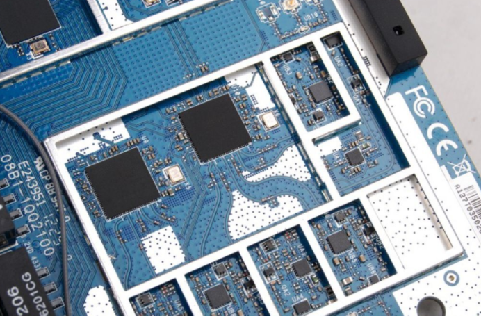
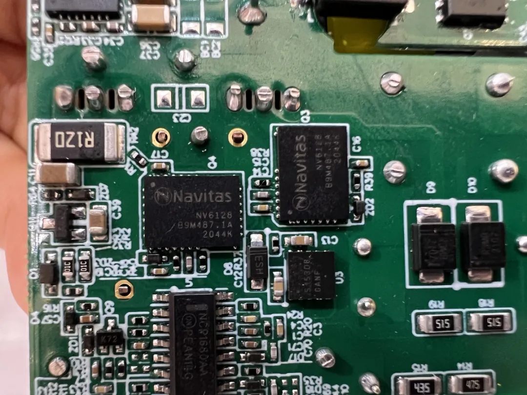
After the blueprint is completed, the next step is PCB design. Design is the layout or physical representation of PCB schematic diagram, including the layout of copper wires and holes. The PCB design shows the location of the above components and their connection to copper.
PCB design is a stage related to performance. Engineers build real components on the basis of PCB design, so that they can test whether the equipment works properly. As we mentioned earlier, anyone should be able to understand the PCB schematic diagram, but it is not easy to understand its function by looking at the prototype.
After these two stages have been completed and you are satisfied with the performance of the PCB, you need to implement them through the manufacturer.
PCB design
PCB schematic elements
After roughly understanding the difference between the two, let's take a closer look at the elements of the PCB schematic. As we mentioned, all connections are visible, but there are some considerations to keep in mind:
In order to see the connections clearly, they are not created in proportion; In PCB design, they may be very close to each other
Some connections may cross each other, which is practically impossible
Some connections may be on the opposite side of the layout, marked to indicate that they are linked
This PCB "blueprint" can use one page, two pages or even several pages to describe all the contents that need to be included in the design
Finally, it should be noted that more complex schematics can be grouped by function to improve readability. The connection arranged in this way will not occur in the next stage, and the schematic is usually inconsistent with the final design of the 3D model.
PCB design elements
Now is the time to go deeper into the elements of PCB design files. At this stage, we move from a written blueprint to a physical representation of the construction using laminate or ceramic materials. When a particularly compact space is required, some more complex applications require the use of Flexible PCBs.
The contents of PCB design documents follow the blueprint formulated by the schematic process, but, as mentioned earlier, they are very different in appearance. We have discussed the PCB schematic, but what differences can be observed in the design file?
When we talk about PCB design documents, we are talking about a 3D model, including PCB and design documents. They can be single or multiple layers, although the most common is two layers. We can observe some differences between PCB schematics and PCB design files:
All PCB components are correct in size and position
If two points should not be connected, you must bypass or switch to another PCB layer to avoid crossing each other on the same layer
In addition, as we briefly mentioned, PCB design pays more attention to actual performance, because this is the verification stage of the final product to some extent. At this point, the design must start to play a role in the practicality of the actual work, and must consider the physical requirements of the printed circuit board. Some of these include:
How the spacing of components allows sufficient heat distribution
Connector on the edge
On current and heat issues, how thick must various traces be
Because physical limitations and requirements mean that PCB design files usually look very different from the design on the schematic, the design files include screen printing layers. The silk screen layer indicates letters, numbers and symbols to help engineers assemble and use the board.
It is required to work as planned after all components are assembLED on the printed circuit board. If not, you need to redraw.


抖音二維碼

Q Q二維碼

微信二維碼
點擊
然后
聯(lián)系
然后
聯(lián)系
電話熱線
13410863085Q Q

微信

- 郵箱