鑫景福致力于滿足“快速服務(wù),零缺陷,輔助研發(fā)”PCBA訂購單需求。


PCBA方案設(shè)計(jì)
The five basIC PCB design specifications we have to look at
For many novices in PCB design, understanding the most basic specifications of PCB design is the first task, which will help develop good PCB design habits and be more suitable for all aspects of electronic manufacturing, such as PCB production, SMT chip processing, DIP plug-in, etc. The following will introduce the five basic specifications in PCB design in great detail.
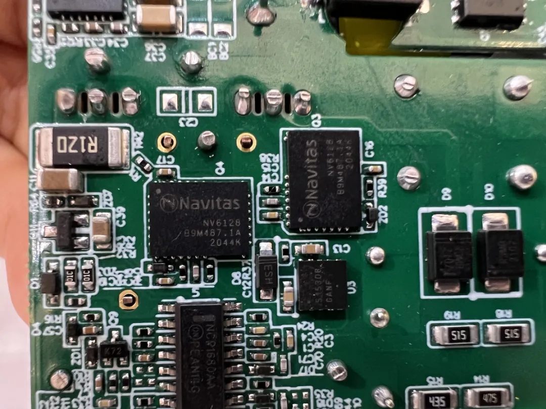
1. Shield cover design
The spacing between the shielding cover and the shielding cover, and between the components in the shielding cover and the shielding cover shall be more than 0.4MM
Cause: At present, the pad width of the shield cover is 0.7MM. In order to reduce the problem of faulty soldering of the shield cover, especially for the shielding covers of models with more and more special-shaped components, the corners of the shield cover are easy to be faulty soldered. At present, the steel MESh width of the shield cover pad will be
0.3MM-0.5MM internal and external reaming treatment
The bonding pad of the shield cover should not be too long, because the bonding pad is too long, which will cause local false soldering after welding with the serration of the shield cover. The length of the bonding pad of the shield cover is designed as 2-2.5MM, one segment at a time, and the sawtooth height is 0.3MM-0.5MM. For the bending part, it is recommended that the bonding pad length should be 1.2-1.5MM as SMAll as possible. The shield cover pin should be made into a sawtooth shape to match the bonding pad.
Cause: At present, the requirement for shield cover manufacturers is that the deformation range is normal at 0.1MM, and the deformation position often occurs at the bend. In combination with our current steel mesh thickness of 0.12MM, it is difficult to grasp the welding effect of the pin, and the larger the pad, the less solder paste on the pad.
2. Pad spacing between PCB devices
The pad spacing between devices should meet the most basic PCB design requirements.
The distance between the discharge tube and the adjacent element PAD is>0.3mm (the distance between the discharge tube and the adjacent element PAD is>0.15mm for the same network and>0.2mm for different networks). The distance between the discharge tube and the discharge tube is>0.1mm
3. Process clamping edge
The distance between the process edge and the top of the board is>5MM (Note: the width of the process clamping edge is 4.5MM when the machine is clamped to the process edge). The width of the process clamping edge is>4MM. During PCB pasting, a certain edge should be reserved for convenient clamping. In this range, it is not allowed to lay components and pads. In case of high-density boards that cannot leave clamping edges, process edges can be designed or the form of panel splicing can be used. Its width depends on the selected SMT equipment. Generally, the process edge is 6.0MM from the top of the component or the edge of the single board, that is, the process edge is more than 5MM from the top of the nearest component or from the inner PCB.
4. MARK point design
For the design of the MARK points of PCB, the MARK points on the same side are designed to be symmetrical (the spacing between the left and right MARK points is the same as that between the board edges), and the upper and lower MARK points are asymmetric (the spacing between the upper and lower MARK points is different from that between the board edges), so as to prevent fooling. The diameter of MARK point on PCB is 1.0MM.
5. Locating hole
The diameter of the positioning hole of the whole panel is 2.5MM+-0.1MM, and the components shall not be placed within 1MM around the positioning hole, so as to avoid extrusion of the components by the support thimble of the panel dividing tooling.
Positioning hole requirements for each panel base plate of single board: current standard: 3.0MM-3.8MM
The above is the basic PCB design specification, which is suitable for beginners and must master and use. In fact, PCB design specifications are far more than these. Designers need to constantly summarize in complex work, take manufacturability and clarity as the basic principles, and ensure that the PCB design documents sent out are accurate, standardized, and clear at a glance. This is also an important aspect of the gap between senior PCB design engineers and beginners.


抖音二維碼

Q Q二維碼

微信二維碼
點(diǎn)擊
然后
聯(lián)系
然后
聯(lián)系
電話熱線
13410863085Q Q

微信

- 郵箱