鑫景福致力于滿足“快速服務,零缺陷,輔助研發”PCBA訂購單需求。


PCBA方案設計
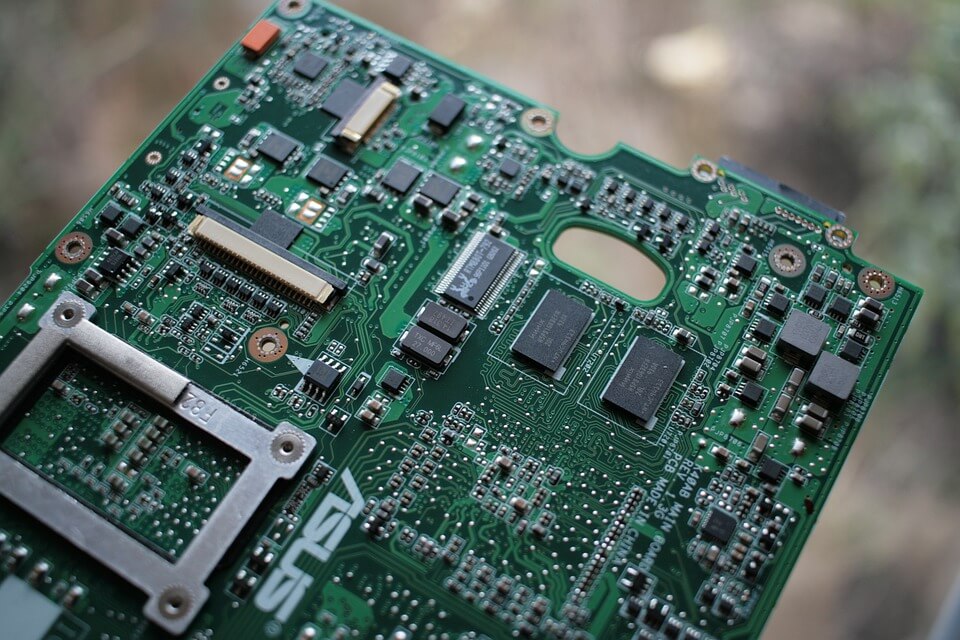
PrintedCircuitboard (PCB), also known as printed circuit board in Chinese, is an important electronIC component, the support body of electronIC components, and the provider of electrical connection of electronic components. Because it is made using electronic printing, it is calLED a "printed" circuit board.
With the requirement of SMAller PCB size and higher device density, PCB design becoMES more and more difficult. How to achieve high PCB routing rate and shorten the design time, the author here to talk about PCB planning, layout and routing design skills.
Before starting wiring, the design should be carefully analyzed and the tool software should be carefully set up, which will make the design more compliant.
1 Determine the number of PCB layers
The size of the circuit board and the number of wiring layers need to be determined at the beginning of the design. The number of wiring layers and stacking mode directly affect the wiring and impedance of cables. The size of the board helps determine the lamination and wiring width to achieve the desired design effect. The cost difference of the current multilayer board is small, and it is better to use more circuit layers and distribute copper evenly at the beginning of the design.
2 Design rules and constraints
To successfully complete the wiring task, the wiring tool needs to work under the correct rules and constraints. Classification of all signal lines with special requirements, each signal class should have a priority, the higher the priority, the more strict the rules. Rules related to wire width, maximum number of through-holes, parallelism, interaction between signal wires, and layer limits have a significant impact on the performance of a wiring tool.
Careful consideration of design requirements is an important step in successful wiring.

3 Component Layout
During optimized assembly, Design for Manufacturability (DFM) rules impose constraints on component layout. If the assembly department allows components to move, the circuit can be properly optimized to make automatic wiring easier. The rules and constraints you define affect the layout design. Autocabling tools consider one signal at a time. By setting constraints on cabling and the number of layers that signal cables can be routed, you can complete the cabling tool as envisioned by the designer.
For example, for the layout of power cables:
(1) In the PCB layout, the power decoupling circuit should be designed near the relevant circuits rather than the power supply. Otherwise, the bypass effect will be affected and the pulse current will flow through the power line and ground wire, causing interference.
(2) The power supply direction inside the circuit should be used from the last stage to the first stage, and the filtering capacitor of this part of the power supply should be close to the final stage layout;
③ For some main current channels, if the current is disconnected or measured in the process of debugging and testing, the current gap should be arranged on the printed wire when the layout.
In addition, pay attention to the layout of the regulated power supply on a separate printed board as much as possible. When the power supply and circuit share a printed board, do not mix the regulated power supply and circuit elements or share the ground wire with the circuit. Because this wiring is not only easy to cause interference, but also can not disconnect the load during maintenance, can only cut off part of the printed wire, thereby damaging the printed board.
4 fan out design
During the fan-out design phase, each pin of the SURface-MOUNT device should have at least one through-hole so that the board can be used for interlayer connections, in-line testing, and circuit remachining when more connections are required.
To maximize the efficiency of the auto-wiring tool, use the largest through-hole size and print line possible, with an optimal interval of 50mil. Use the type of through-hole that maximizes the number of wiring paths. After careful consideration and prediction, the design of circuit online testing can be carried out early in the design and implemented later in the production process.
The type of through-hole fan out is determined according to the wiring path and the circuit online test. Power supply and grounding also affect wiring and fan-out design.
5 Key signals and manual cabling
Manual wiring is an important process in PCB design now and in the future. Manual wiring helps automatic wiring tools to complete the wiring work.
By manually wiring and fixing the selected network (net), a path can be formed that can be used for automatic wiring.
First, route key signals manually or in combination with automatic routing tools. After the wiring is complete, the relevant engineering and technical personnel shall check the wiring of these signals. When the check passes, fix these cables and start to automatically wire the remaining signals.
Because of the impedance in the ground wire, it will bring common impedance interference to the circuit. Therefore, when wiring, do not randomly connect any point with ground symbol, which may cause harmful coupling, affect the work of the circuit.
At higher frequencies, the inductive reactance of the wire will be orders of magnitude greater than the resistance of the wire itself. At this time, even if only a small high-frequency current flows through the wire, it will produce a certain high-frequency voltage drop. Therefore, for high-frequency circuits, the PCB layout should be as compact as possible and the wiring should be as short as possible.
There is mutual inductance and capacitance between printed wires. When the working frequency is high, it will cause interference to other parts, which is called parasitic coupling interference. Suppression methods can be taken as follows:
(1) Shorten the signal routing between all levels as far as possible;
(2) Arrange all levels of circuits according to the signal sequence to prevent all levels of signal lines from crossing each other;
(3) The wires of the adjacent two panels should be vertical or horizontal. Cross, not parallel;
(4) When the signal cables are arranged in parallel in the board, they should be separated from each other as far as possible, or the ground cables and power cables should be separated to achieve the purpose of shielding.
6 Automatic Cabling
The routing of key signals should be considered to control some electrical parameters during the routing, such as reducing the distributed inductance. After understanding the input parameters of the automatic routing tool and the influence of the input parameters on the routing, the quality of the automatic routing tool can be guaranteed to a certain extent.
General rules should be used when automatically wiring signals. By setting constraints and cable-free areas to limit the number of layers used for a given signal and the number of through-holes used, the cabling tool can automatically route the wires according to the engineer's design thinking. After setting the constraints and applying the created rules, the automatic wiring will achieve SIMilar results as expected, and after part of the design is completed, it will be fixed to prevent it from being affected by the subsequent wiring process.
The number of trails depends on the complexity of the circuit board and how many general rules are defined. Today's automated routing tools are so powerful that they can often do 100 percent of the wiring. However, when the automatic wiring tool has not finished wiring all the signals, the remaining signals need to be wired manually.
7 Cable Layout
Some less constrained signals, the length of the line is very long. At this time, you can first judge which wiring is reasonable and which wiring is not reasonable, and then shorten the length of signal wiring by manual editing to reduce the number of holes.
Design of High Speed PCB Based on PROTEL
11-01,2022


抖音二維碼

Q Q二維碼

微信二維碼
點擊
然后
聯系
然后
聯系
電話熱線
13410863085Q Q

微信

- 郵箱