鑫景福致力于滿足“快速服務,零缺陷,輔助研發”PCBA訂購單需求。


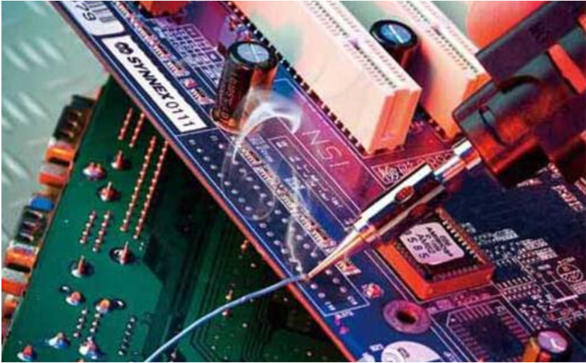
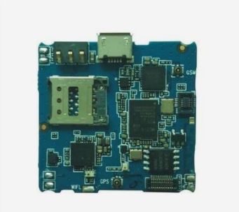
PCBA方案設計
Although there are many disputes about the value, definition, variability and technology of PCB DFM design, all the problems are based on chips. Of course, when we start to consider 45 and 32 nanometer designs, chip DFM is a key requirement. However, we pay attention to the chip DFM, but ignore the more important technICal needs: the printed circuit board oriented DFM.

We all know that even if the silicon chip is 100% perfect, if any component of the chip to chip communication link (such as package, connector or circuit board) is damaged, the target system may still not work properly. Many packaging, connector, and PCB suppliers may be pushed by system designers to control their processing tolerances.
However, unless all PCB suppliers uniformly strengthen the specification, for example, a connector with a tolerance of plus or minus 5% may have little effect on a system with a tolerance of plus or minus 10% for PCB. In order to optimize the system design, designers need to study the causal relationship of each component. So far, we do not have DFM tools to deal with such design problems.
In the PCB pre layout design phase, high-speed system or signal integrity engineers usually can only conduct limited SPIce SIMulation. To ensure the normal operation of the system, it is necessary to simulate the boundary conditions that can cover all machining tolerances.
For example, changes in metal line width, dielectric stack height, dielectric constant and loss tangent value in PCB can all affect impedance and attenuation. However, only engineers of large companies can have the resources to customize their own scripts to perform thousands of simulation tasks, and then process the results. Even so, there is still no well-defined standard for which variables to scan.
The most obvious lack is the boundary model of encapsulation and connector. For high-speed design, these models can only be precisely defined by frequency related S parameters. However, few suppliers provide good S parameter models, let alone boundary models in a wide range of frequencies.
In the post layout verification phase, complex PCB needs to be accurately extracted and simulated to calculate detaiLED corners and bends. However, few tools are available.
Obviously, a general PCB design and verification method is required. So, what do we need?
Let's focus on two areas. For pre layout design, for example, it is better to have a GUI driven circuit diagram input editor, so that designers can easily input the changes of each component, simulate and process the results, and report the generation and impact of each variable.
For post layout verification, DFM tools need to be able to automatically adjust the layout to cover the boundary situation, use a fast full wave extractor to extract parasitic parameters, and use I/O transistor boundary model in circuit simulation.
Only when PCB designers have considered the work difference in the design and verification can they say they have done the design for manufacturability. Only when the tool supplier realizes that the chip is only a part of the subsystem, such as PCB, can DFM finally be truly relevant to the customer developing the terminal product.


抖音二維碼

Q Q二維碼

微信二維碼
點擊
然后
聯系
然后
聯系
電話熱線
13410863085Q Q

微信

- 郵箱