鑫景福致力于滿足“快速服務,零缺陷,輔助研發”PCBA訂購單需求。


PCBA方案設計
Pcb factory explained: PCB copy, SIMplified process of PCB design
The design of printed circuit board is based on the circuit schematIC diagram to realize the functions required by the circuit designer. The design of printed circuit board mainly refers to layout design, which needs to consider the layout of external connections. The optimal layout of internal electronIC components, the optimal layout of metal wiring and through-hole, electromagnetic protection, heat dissipation and other factors. Excellent layout design can save production costs and achieve good circuit performance and heat dissipation. Simple layout design can be realized by hand, while complex layout design needs to be realized by computer aided design (CAD).
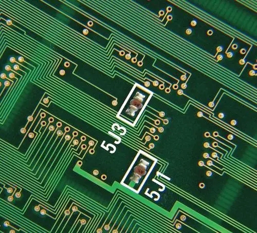
In PCB, special components refer to the key components in the high-frequency part, the core components in the circuit, the components susceptible to interference, the components with high voltage, the components with high heat, and some heterosexual components. The positions of these special components need to be carefully analyzed, and the tape layout should meet the requirements of circuit functions and Production requirements. Improper placement of them may cause circuit compatibility problems and signal integrity problems, which may lead to PCB design failure.
The size of PCB shall be considered first when placing special components in the design. Quick buy points out that when PCB size is too large, the printing line is long, the impedance increases, the dry resistance decreases, and the cost increases; If it is too SMAll, the heat dissipation is poor, and adjacent lines are easily disturbed. After determining the size of PCB, determine the swing position of special components. Finally, all components of the circuit are arranged according to the functional unit. The location of special components shall generally comply with the following principles:
1. Shorten the connection between high-frequency components as much as possible, and try to reduce their distribution parameters and mutual electromagnetic interference. Components susceptible to interference shall not be too close to each other, and the input and output shall be as far away as possible.
2 Some components or wires may have high potential difference, so their distance shall be increased to avoid accidental short circuit caused by discharge. High voltage components should be kept out of reach.
3. Components weighing more than 15G can be fixed with brackets and then welded. Those heavy and hot components should not be placed on the circuit board, but on the bottom plate of the main box, and heat dissipation should be considered. Thermal components shall be far away from heating components.
4. For the layout of adjustable components such as potentiometers, adjustable inductance coils, variable capacitors, microswitches, etc., the structural requirements of the whole board should be considered. Some switches that are often used should be placed in places that are easy to reach when the structure allows. The Layout of components should be balanced, and the density should be appropriate.
For the success of a product, the first is to pay attention to the internal quality. The second is to give consideration to the overall beauty. Only a perfect board can become a successful product.
Step 1: Open the network table (some editors can be used to assist editing)
Browse the package of components in the process of PCB design and PCB copy to ensure that the package of all components is correct and the package of all components is included in the component library. All information in the network table is capitalized, and problems are loaded at the same time, or the BOM list of PCB is discontinuous. For the specific naming rules of components, please refer to the Packaging Naming Rules for Common Components of Suzhou Silicon Technology Co., Ltd. Remember that all components in PCB design and PCB copying process are packaged in the company's unified component library. For packages that do not exist in the component library, the hardware engineer should provide the component DATASHEET or the physical object should be built by a specially assigned person and the other party should confirm.
Step 2: Create PCB PCB frame
First, create PCB PCB files according to PCB design and PCB Layout structure diagram, or corresponding templates, including relevant information such as mounting holes and prohibited layout areas. The key is to MARK the dimensions during PCB design and PCB copying. The precise structure of PCB shall be indicated in the drilling layer, and no closed dimension can be formed.
Step 3: Load the network table during PCB design and PCB copy
The first task is to eliminate problems, load the netlist and eliminate all loading problems. For details, see the PROTEL Technical Manual. Other software loading problems have many similarities, which can be used for reference. If PROTEL is used, the netlist must be loaded more than twice (without any prompt MESsage) to confirm that the netlist is loaded correctly.


抖音二維碼

Q Q二維碼

微信二維碼
點擊
然后
聯系
然后
聯系
電話熱線
13410863085Q Q

微信

- 郵箱