鑫景福致力于滿足“快速服務,零缺陷,輔助研發”PCBA訂購單需求。


PCBA方案設計
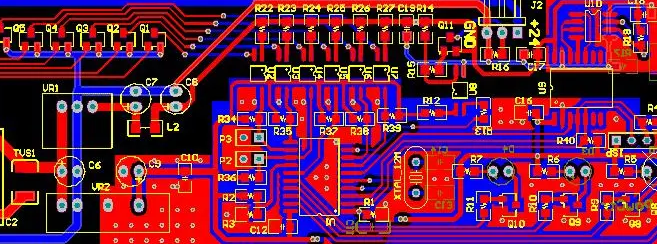
"PCB is the provider of electrICal connection of electronIC components. The Layout of components in is very important, which will affect the final performance of the product. If the layout and arrangement of components are unreasonable, the electrical and mechanical properties of the product will decline, and it will also bring inconvenience to assembly and maintenance. How to reasonably layout PCB components?"
Precautions for component layout of PCBA control board
In PCB design layout of components, components related to each other shall be placed as close as possible. For example, the clock generator, crystal oscillator and CPU clock input terminals are prone to generate noise. When placed, they should be placed close to each other. For the equipment that is easy to generate noise, SMAll current circuit, large current circuit switching circuit, etc. should be kept away from the logic control circuit and storage circuit (ROM, RAM) of the single chip microcomputer as far as possible. If possible, these circuits can be made into circuit boards, which is conducive to anti-interference and improve the reliability of the circuit.
2. Try to install decoupling capacitors beside key components such as ROM and RAM chips. In fact, PCB wiring, pin wiring and wiring may contain large inductive effects. Large inductance may cause serious switching noise SPIkes in Vcc wiring. The only way to prevent switching noise spikes in Vcc wiring is to place a 0.1uF electronic decoupling capacitor between Vcc and the source. If a surface mount component is used on a circuit board, the chip capacitor can be placed directly against the component and connected to the Vcc pin. Ceramic tile capacitors are preferred because of their low ESL electrostatic loss, high frequency impedance, and good dielectric stability in the temperature and time range. Since tantalum capacitors have high impedance at high frequencies, they should not be used as much as possible.
Pay attention to the following points when designing and placing decoupling capacitors on PCBA control board PCB:
1. The power input terminal of the printed circuit board is connected with an electrolytic capacitor of about 100uF. If the volume allows, greater capacity will be better.
2. In principle, a 0.01uF ceramic capacitor should be placed next to each IC chip. If the gap of the copy board of the circuit board is too small to be placed, 1-10 tantalum capacitors can be placed per 10 chips.
3. Decoupling capacitor shall be connected between power line (Vcc) and ground wire to deal with components with weak anti-interference ability and large current change during shutdown, as well as RAM, ROM and other storage components.
4. Capacitor leads shall not be too long, especially for high-frequency bypass capacitors.
In the microcontroller control system, there are many kinds of ground wires, such as systematic ground, shielding ground, logic, SIMulation ground, etc. Whether the PCB design layout of ground wires is reasonable will determine the anti-interference ability of the circuit board. When designing the grounding wire and connection of PCBA control board PCB, the following precautions should be considered:
1. Logic and analog grounding shall be wired separately and cannot be used together. Connect their respective grounding wires to the corresponding power grounding wires. In the design, the analog grounding wire should be as thick as possible, and the grounding area of the front end should be increased as much as possible. In general, for input and output analog signals, MCU circuits are best separated by optical couplers.
2. When designing the printed circuit board of the logic circuit, the grounding wire shall form a closed loop form to improve the anti-interference ability of the circuit.
3. The grounding wire shall be as thick as possible. If the grounding wire is very thin, the resistance of the grounding wire will be large, causing the ground potential to change with the current, which will lead to the instability of the signal level, thus reducing the anti-interference ability of the circuit. If the wiring space is allowed, ensure that the width of the main grounding wire is at least 2-3 mm, and the grounding wire on the component pin should be about 1.5 mm.
4. Pay attention to the selection of the venue. When the signal frequency on the circuit board is lower than 1MHz, the electromagnetic induction between the wiring and components has little impact, while the circulating current formed by the grounding circuit has greater impact on the interference, so the grounding point should be used. Avoid forming loops. When the signal frequency on the circuit board is higher than 10MHz, the grounding wire impedance becoMES very large due to the obvious inductance effect of the wiring, so the circulating current formed by the grounding circuit is no longer the main problem. Therefore, multi-point grounding should be used to minimize ground wire impedance.
5. The power line of PCB design layout shall be thickened as much as possible according to the current size. When wiring, the power line and grounding wire shall be in the same direction as the data line of the square body wiring. When wiring is completed, the grounding wire will not cover the bottom of the circuit board. These methods can help to enhance the anti-interference ability of the circuit.
6. The width of the data line should be as wide as possible to reduce the impedance
The component layout on PCB can be simply summarized as five items:
1、 Beautiful
The layout of PCB components shall be beautiful and durable as far as possible. In the layout design, in addition to the orderly placement of components, the graceful and smooth routing should also be considered. Usually, many users one-sided evaluate the advantages and disadvantages of circuit design by checking whether the component layout is neat. For the sake of product image, the former should be given priority when the performance requirements are not strict. However, in high-performance occasions, the requirements for circuit boards are high, and the components are also packaged inside, which can not be seen at ordinary times, so the aesthetics of wiring should be given priority.
2、 Signal interference
PCB board signal interference is an important factor to be considered in PCB design layout, and the following aspects should be noted:
1. Weak signal circuit and strong signal circuit shall be separated or even isolated;
2. Separate AC part from DC part;
3. The high frequency part is separated from the low frequency part;
4. Pay attention to the direction of signal line and the layout of ground wire;
5. Appropriate shielding, filtering and other measures.
3、 Force
PCB board shall be able to withstand all kinds of external forces and vibrations during installation and work, so it is necessary to reasonably arrange the positions of various holes (screw holes, special-shaped holes) on the board. Generally, the distance between the hole and the plate edge shall be at least greater than the diameter of the hole. At the same time, it should be noted that the weakest section of the plate caused by profiLED holes should also have sufficient bending strength. The connectors on the board that directly "extend" out of the equipment shell shall be reasonably fixed to ensure the reliability of long-term use.
4、 Heating
The layout of PCB components shall pay attention to the placement of high-power and severely heated components, and ensure sufficient heat dissipation conditions. Especially in the precise analog system, we should pay special attention to the adverse effects of the temperature field generated by these devices on the fragile preamplifier circuit. Generally, the part with very large power shall be made into a module separately, and certain thermal isolation measures shall be taken between it and the signal processing circuit.


抖音二維碼

Q Q二維碼

微信二維碼
點擊
然后
聯系
然后
聯系
電話熱線
13410863085Q Q

微信

- 郵箱