鑫景福致力于滿足“快速服務(wù),零缺陷,輔助研發(fā)”PCBA訂購單需求。


PCBA方案設(shè)計
With the rapid development of electronIC technology, PCB manufacturerscan find a way out in the highly competitive PCB industry only by actively developing and innovating production technology on the basis of recognizing the development trend of PCB technology. Circuit board manufacturers should always keep a sense of development. The following are some views on the development of PCB production and processing technology in Changsha:
Develop component embedding technology
Component embedding technology is a huge change in PCB functional integrated circuits. The formation of semiconductor devices (calLED active components), electronIC components (called passive components) or passive component functions "component embedded PCB" in the inner layer of PCB has begun to be mass produced. However, to develop circuit board manufacturers, they must first solve the SIMulation design method, and the production technology and inspection of quality and reliability assurance are also urgent. It is necessary to increase resource investment in systems including design, equipment, detection and simulation to maintain strong vitality.
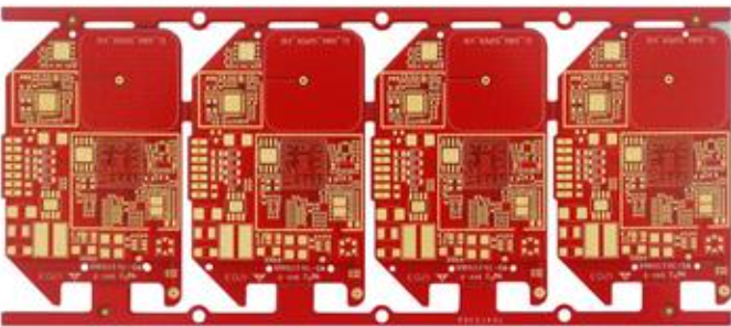
Several Trends of PCB Technology Development and Innovation in Pcb factory
2. HDI technology is still the mainstream development direction
Technology promotes the development of mobile phones, LSI and CSP chips (packaging) for information processing and control of basic frequency functions, and template substrates for circuit board packaging. It also promotes the development of PCB. Therefore, Circuit board manufacturers should innovate PCB production and processing technology along the HDI road. As HDI embodies the most advanced technology of contemporary PCB, it brings fine wiring and micro aperture to PCB. Mobile phone (mobile phone), one of the electronic products of HDI Multilayer board application terminal, is a model of HDI's cutting-edge development technology. In the mobile phone, the PCB main board fine wire (50 μ m~75 μ m/50 μ m~75 μ m. Conductor width/spacing) has become the mainstream, in addition, the thickness of conductive layer and plate is thin; The miniaturization of conductive patterns brings high-density and high-performance electronic equipment.
3. Continuously introduce advanced production facilities and update circuit board manufacturing process
HDI manufacturing has become mature and tends to be perfect. With the development of PCB technology, although the manufacturing methods commonly used in the past are still dominant, low-cost processes such as additive and sEMI additive have begun to emerge. Using nanotechnology to metallize holes and form PCB conductive patterns at the same time, a new flexible board manufacturing process is developed. High reliability, high quality printing method, ink-jet PCB technology. Production of fine wires, new high-resolution photomask and exposure devices, and laser direct exposure devices. Uniform coating equipment. Manufacturing and installation equipment and facilities for embedded production components (passive active components).
Several Trends of PCB Technology Development and Innovation in PCB Factory
4. Develop PCB raw materials with higher performance
Whether rigid PCB or flexible PCB materials, with the lead-free global electronic products, it is required to make these materials have higher heat resistance. Therefore, new materials with high Tg, SMAll coefficient of thermal expansion, small dielectric constant and better dielectric loss than tangent are emerging.
5. Photoelectric PCB has broad prOSPects
Photoelectric PCB circuit board uses optical path layer and circuit layer to transmit signals. The key of this new technology is to manufacture optical path layer (optical waveguide layer). It is an organic polymer, which is formed by means of lithography, laser ablation, reactive ion etching, etc. At present, the technology has been industrialized in Japan and the United States. As a large country of production, Chinese circuit board manufacturers should also actively respond and keep pace with the development of science and technology.


抖音二維碼

Q Q二維碼

微信二維碼
點擊
然后
聯(lián)系
然后
聯(lián)系
電話熱線
13410863085Q Q

微信

- 郵箱