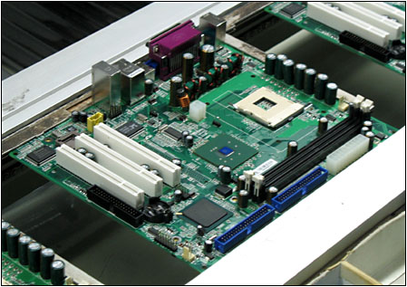
鑫景福致力于滿足“快速服務(wù),零缺陷,輔助研發(fā)”PCBA訂購單需求。


PCBA方案設(shè)計

The stacking arrangement of PCB factoryis the basis of the whole system. If the stack design is defective, it will eventually affect the EMC performance of the whole machine. In general, the stack design mainly follows two rules:
1. Each routing layer must have an adjacent reference layer (power supply or stratum);
2. The adjacent main power supply layer and stratum shall be kept at a minimum distance to provide large coupling capacitance;
The following lists the laminations from single ply to eight ply panels:
1 Lamination of single panel and double panel
For two-layer plates, there is no stacking problem due to the SMAll number of plates. The control of EMI radiation is mainly considered from PCB wiring and PCB layout;
The electromagnetic compatibility problem of single-layer board and double-layer board is more and more prominent. The main reason for this phenomenon is that the signal loop area is too large, whICh not only generates strong electromagnetic radiation, but also makes the circuit sensitive to external interference. The SIMplest way to improve the electromagnetic compatibility of lines is to reduce the loop area of key signals.
Key signals: from the perspective of electromagnetic compatibility, key signals mainly refer to signals that generate strong radiation and are sensitive to the outside world. Signals that can generate strong radiation are generally periodic signals, such as clock or address low order signals. Signals sensitive to interference refer to those analog signals with low level.
Single and double layer boards are usually used in low frequency analog design below 10KHz:
1 The power supply lines on the same floor shall be arranged in a radial manner, and the total length of the lines shall be minimized;
2 When running the power supply and ground wire, they should be close to each other; Lay a ground wire beside the key signal line, which shall be as close to the signal line as possible. In this way, a smaller loop area is formed to reduce the sensitivity of differential mode radiation to external interference. When a ground wire is added beside the signal wire, a loop with the smallest area is formed, and the signal current will definitely pass through this loop rather than other ground wire paths.
3 If it is a double-layer circuit board, a ground wire can be laid along the signal line on the other side of the circuit board, close to the bottom of the signal line, and the line should be as wide as possible. The loop area thus formed is equal to the thickness of the pcb circuit board tiMES the length of the signal line.
2 Lamination of four layers
Recommended stacking method:
2.1 SIG-GND(PWR)-PWR (GND)-SIG;
2.2 GND-SIG(PWR)-SIG(PWR)-GND;
For the above two kinds of circuit board stack designs, the potential problem is the traditional 1.6mm (62mil) board thickness. The layer spacing will become very large, which is not only bad for impedance control, interlayer coupling and shielding; In particular, the large spacing between the power supply layers reduces the capacitance of the board, which is not conducive to filtering noise.
For the first scheme, it is usually applied to the situation where there are many chips on the board. This scheme can achieve good SI performance, but it is not very good for EMI performance. It is mainly controlLED by routing and other details. Note: The stratum is placed at the connecting layer of the signal layer with the most dense signals, which is conducive to absorbing and suppressing radiation; Increase the plate area to reflect the 20H rule.
For the second scheme, it is usually applied to the situation where the chip density on the board is low enough and there is enough area around the chip (to place the required power supply copper coating). In this scheme, the outer layer of PCB is stratum, and the middle two layers are signal/power layers. The power supply on the signal layer is routed with a wide wire, which can make the path impedance of the power supply current low and the impedance of the signal microstrip path low, and can also shield the signal radiation of the inner layer through the outer layer. From the perspective of EMI control, this is the best 4-layer PCB structure available. Main note: the distance between the signal and power mixing layers of the middle two layers shall be extended, and the wiring direction shall be vertical to avoid crosstalk; Appropriate control panel area, reflecting the 20H rule; If the routing impedance is to be controlled, the above scheme should be very careful to arrange the routing under the power supply and grounding copper island. In addition, the copper laying on the power supply or stratum shall be interconnected as much as possible to ensure the connectivity of DC and low frequency.
PCB design
3 Lamination of six layers
For the design with high chip density and high clock frequency, 6-layer Board Design should be considered
Recommended stacking method:
3.1 SIG-GND-SIG-PWR-GND-SIG;
For this scheme, this stacking scheme can obtain good signal integrity. The signal layer is adjacent to the ground layer, and the power layer and the ground layer are paired. The impedance of each routing layer can be well controlled, and both layers can well absorb magnetic lines of force. And it can provide a better return path for each signal layer when the power supply and stratum are complete.
3.2 GND-SIG-GND-PWR-SIG -GND;
For this scheme, this scheme is only applicable to the case where the device density is not very high. This kind of lamination has all the advantages of the upper lamination. In addition, the ground surfaces of the top layer and the bottom layer are relatively complete and can be used as a better shielding layer. It should be noted that the power supply layer should be close to the layer of non main component, because the plane of the bottom layer will be more complete. Therefore, EMI performance is better than the first scheme.
Summary: For the Six layer board scheme, the spacing between the power supply layer and the stratum should be minimized to obtain good power and ground coupling. However, with the thickness of 62mil, it is not easy to control the distance between the main power supply and the stratum very small, although the layer spacing is reduced. Compared with the first scheme and the second scheme, the cost of the second scheme will be greatly increased. Therefore, we usually choose the first scheme when stacking. During design, follow 20H rules and mirror layer rules
4 Lamination of eight layers
The following three stacking methods are usually used for the eight ply board
4.1 This is not a good stacking method due to poor electromagnetic absorption capacity and large power impedance. Its structure is as follows:
1 Signal 1 component surface, microstrip routing layer
2 Signal 2 internal microstrip routing layer, good routing layer (X direction)
3 Ground
4 Signal 3 stripline routing layer, good routing layer (Y direction)
5 Signal 4 stripline routing layer
6 Power
7 Signal 5 Internal Microstrip Routing Layer
8 Signal 6 Microstrip Routing Layer
4.2 is a variation of the third stacking method. Due to the addition of reference layer, it has good EMI performance, and the characteristic impedance of each signal layer can be well controlled
1 Signal 1 component surface, microstrip routing layer, good routing layer
2 Ground formation, good electromagnetic wave absorption capacity
3 Signal 2 ribbon line routing layer, good routing layer
4 Power layer, which forms excellent electromagnetic absorption with the stratum below
5 Ground stratum
6 Signal 3 ribbon line routing layer, good routing layer
7 Power stratum, with large power impedance
8 Signal 4 Microstrip routing layer, good routing layer
4.3 The best stacking mode, due to the use of multi-layer ground reference plane, has very good geomagnetic absorption capacity.
1 Signal 1 component surface, microstrip routing layer, good routing layer
2 Ground formation, good electromagnetic wave absorption capacity
3 Signal 2 ribbon line routing layer, good routing layer
4 Power layer, which forms excellent electromagnetic absorption with the stratum below
5 Ground stratum
6 Signal 3 ribbon line routing layer, good routing layer
7 Ground formation, good electromagnetic wave absorption capacity
8 Signal 4 Microstrip routing layer, good routing layer
5、 Summary
How to select the number of layers and the stacking method for design depends on many factors such as the number of signal networks on the circuit board, device density, PIN density, signal frequency, board size, etc. We should consider these factors comprehensively. The more the number of signal networks, the greater the device density, the greater the PIN density, and the higher the signal frequency, the design should try to use multilayer PCB boards. In order to obtain good EMI performance, it is best to ensure that each signal layer has its own reference layer.


抖音二維碼

Q Q二維碼

微信二維碼
點擊
然后
聯(lián)系
然后
聯(lián)系
電話熱線
13410863085Q Q

微信

- 郵箱