鑫景福致力于滿足“快速服務,零缺陷,輔助研發”PCBA訂購單需求。


PCBA方案設計
In the pcb design, we only need to pull lines in addition to PCB layout, so what are the requirements for outgoing lines? They are not random. Let's learn together!
1. In order to meet the requirements of doMEStIC production process capacity, the width of conventional wiring is ≥ 4mil (0.1016mm) (3.5mil, i.e. 0.0889mm in special cases); Less than this value will greatly challenge the production capacity of PCB factories and improve the scrap rate.
2. The wire cannot be routed at any angle to challenge the manufacturer's production capacity. Many problems occur when etching copper wires. It is recommended to route at 45 ° or 135 °.
3. The same network should not be routed at 90 ° right angle or acute angle, which is generally a situation that should be avoided as much as possible in PCB wiring, and it has almost become one of the standards to measure the quality of PCB wiring. Right angle routing will change the line width of transmission lines, cause impedance discontinuity, cause signal reflection, and cause EMI at the tip to affect the line.
4. The shape of pads is generally regular, such as BGA pads are round, QFP pads are oblong, chip pads are rectangular, etc. However, the actually made PCB and PCB pad are irregular, which can be said to be grotesque. Take R0402 resistance encapsulated pads as an example. After regular pads are wired out, the process deviation during production will become an actual pad, which is composed of a SMAll rectangular pad added to the original rectangular pad. Irregular pads are wired out.
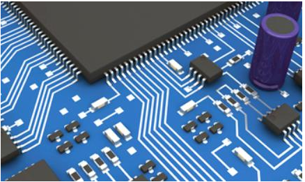
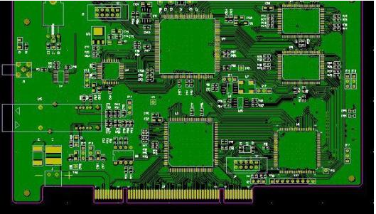
PCB design outlet
In PCB design, if the two pads of 0402 resistor package are wired diagonally, plus the solder resistance deviation caused by the PCB production precision (the solder resistance window is 0.1mm larger than the pad on one side), the solder pad shown will be formed. In this case, bad rotation will occur due to the effect of solder surface tension during resistance welding.
Reasonable wiring mode and fanout mode about long axis symmetry are adopted for bonding pad connection, which can effectively reduce the bad rotation of chip components after mounting. If the lines fanned out by the pad are also symmetrical about the short axis, the drift of CHIP components after mounting can also be reduced.
5. Adjacent pads are the same as the network and cannot be directly connected. You need to connect the pads first and then connect them. Straight chains are easy to cause continuous welding during manual welding.
6. The connector teaching cable needs to be pulLED out from the center of the PCB pad and then moved outward. No other angle is allowed to avoid tearing the cable when the connector is plugged in.
After learning these specifications, do you have a deeper understanding of PCB cable? Now apply them to your own projects!


抖音二維碼

Q Q二維碼

微信二維碼
點擊
然后
聯系
然后
聯系
電話熱線
13410863085Q Q

微信

- 郵箱