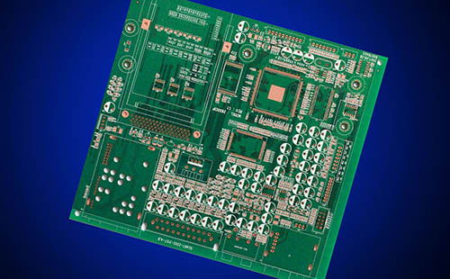
鑫景福致力于滿足“快速服務,零缺陷,輔助研發”PCBA訂購單需求。


PCBA方案設計
The electronICs manufacturer explains the second half of the PCB design process
1.6 Recheck
Recheck according to "PCB checklist", including design rules, layer definition, line width, spacing, pad and via settings.
The rationality of the device layout, the routing of the power supply and ground network, the routing and shielding of the high-speed clock network, the placement and connection of the decoupling capacitor, etc. shall also be rechecked. If the recheck is unqualified, the designer shall modify the layout and wiring. After the recheck is qualified, the reviewer and the designer shall sign respectively.
1.7 Design output
PCB design can be output to printer or photo file The printer can print PCB layer by layer, which is convenient for designers and reviewers to check; The photo drawing documents shall be submitted to the board manufacturer to produce printed boards The output of photo files is very important, which is related to the success or failure of this design. The following will focus on the precautions for outputting photo files.
A. The layers to be output include wiring layer (including top layer, bottom layer and intermediate wiring layer), power layer (including VCC layer and GND layer), silk screen layer (including top layer silk screen and bottom layer silk screen), solder mask layer (including top layer solder mask and bottom layer solder mask), and also generate drilling file (NC Drill).
b. If the power supply layer is set to Split/Mixed, select Routing in the Document item of the Add Document window, and use the Plane Connect of Pour Manager to copper-clad PCB drawings before outputting photo files each time; If it is set to CAM Plane, select Plane. When setting Layer, add Layer25, and select Pads and Viasc in Layer25 In the device setup window (press Device Setup), change the Aperture value to 199.
d. When setting the Layer of each layer, select Board Outline.
e. When setting the layer of the silk screen layer, do not select the Part Type, but select the Outline, Text and Line of the top layer (bottom layer) and silk screen layer.
f. When setting the layer of the solder mask layer, selecting via means that there is no solder mask on the via, and not selecting via means that there is solder mask on the via, depending on the specific situation.
g. When generating drilling files, use the default settings of PowerPCB and do not make any changes.
h. After all photo files are output, open them with CAM350 and print them. Designers and reviewers check vias (via) according to the "PCB checklist", which is one of the important components of multilayer PCBs. Drilling costs usually account for 30 to 40 percent of PCB manufacturing costs. In short, each hole on a PCB can be calLED a via. From the perspective of function, vias can be divided into two categories:
First, it is used as the electrical connection between layers;
The other is used for fixing or positioning devices In terms of process, these vias are generally divided into three categories, namely blind via, buried via and through via The blind hole is located on the top and bottom surfaces of the printed circuit board, and has a certain depth. It is used to connect the surface line and the inner line below. The depth of the hole usually does not exceed a certain ratio (aperture). The buried hole refers to the connection hole located on the inner layer of the printed circuit board, which does not extend to the surface of the printed circuit board The above two types of holes are located in the inner layer of the circuit board. Before lamination, the through hole forming process is used to complete the hole. During the hole forming process, several inner layers may be overlapped.
The third is called through hole, which passes through the whole circuit board and can be used for internal interconnection or as the installation and positioning hole of components Because the through hole is easier to realize in technology and lower in cost, most printed circuit boards use it instead of the other two kinds of through holes. The following through holes, unless otherwise specified, are considered as through holes From the design point of view, a via is mainly composed of two parts: one is the drill hole in the middle, and the other is the pad area around the drill hole, as shown in the figure below. The size of these two parts determines the size of the via.
Obviously, when designing high-speed and high-density PCBs, designers always hope that the SMAller the vias are, the better, so that more wiring space can be left on the board. In addition, the smaller the vias are, the smaller their parasitic capacitance is, which is more suitable for high-speed circuits However, the reduction of hole size also brings about an increase in cost, and the size of vias cannot be reduced without limitation. It is limited by drilling, plating and other technologies: the smaller the hole, the longer it takes to drill, and the easier it is to deviate from the center; When the depth of the hole exceeds 6 tiMES of the drilling diameter, it is impossible to ensure that the hole wall can be uniformly copper plated For example, the thickness (through-hole depth) of a normal 6-layer PCB is about 50Mil, so the minimum drilling diameter that PCB manufacturers can provide can only reach 8Mil.


抖音二維碼

Q Q二維碼

微信二維碼
點擊
然后
聯系
然后
聯系
電話熱線
13410863085Q Q

微信

- 郵箱