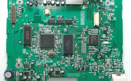
鑫景福致力于滿足“快速服務(wù),零缺陷,輔助研發(fā)”PCBA訂購單需求。


PCBA方案設(shè)計(jì)
ApplICation Scheme and Advantages of PlaSMA Technology in PCB Manufacturing
Whether it is military aerOSPace communications or civil consumer electronics, the demand for high-performance PCB circuit boards is growing due to the increasingly diversified functions and high reliability requirements; Therefore, the high-density and fine circuit design and the application of new materials make the PCB manufacturing process more complex and challenging. Plasma processing technology is gradually recognized by PCB manufacturers and replaces chEMIcal or mechanical processing methods with its obvious advantages to meet today's increasingly stringent PCB manufacturing process requirements.
Compared with traditional chemical wet treatment, plasma treatment has the following advantages:
1. The process is controllable; Good consistency and repeatability
2. Strong permeability to fine lines, micropores and products with high thickness diameter ratio
3. Wide range of applications, can handle various materials including PTFE, LCP and other chemical resistant special materials
4. Economical and environmental protection, no need for chemical solvents, no waste disposal requirements
Plasma is a partially ionized gas, which is composed of a large number of active groups, including electrons, ions, free radicals and photons (UV and visible light). It is often regarded as the fourth state of matter except solid, liquid and gas states. Because the number of positive and negative particles is equal and electrically neutral, it is calLED "plasma". Plasma treatment mainly has two reaction mechanisms: chemical reaction formed by free radicals and by-products and physical bombardment generated by ions. Two reaction mechanisms, depending on the gas type and plasma mode, can be applied to different PCB manufacturing process applications:
1. DeSMEar
2. Etch Back Erosion
3. Carbon removal (laser blind hole bottom cleaning)
4. PTFE Activation
5. Remove dry film/green oil residue between Descum fine lines
6. Surface oxidation removal and activation to improve metal sputtering/weldability
7. Surface modification (roughening and activation):
a) Treatment before reinforcement
b) Lamination pretreatment
c) Anti welding pretreatment
d) Silk screen character pre-processing
e) Improve surface wettability and improve material coatability
The main indicators of plasma treatment process in PCB manufacturing are etching rate (glue removal rate) and uniformity (consistency). The uniformity is evaluated by weighing or slicing, including between boards (cavity), inside boards, and inside holes (orifice and middle of holes). It depends on the overall design of the equipment, and is also closely related to plasma process parameters, including power, gas selection and flow, vacuum, temperature control, etc. The V30 series plasma machine developed for PCB manufacturing applications is used for PCB production with high process requirements such as HDI, high thickness diameter ratio (>20:1), PTFE high-frequency communication, backplane, server board, and is highly praised for its reliable quality, fast glue removal rate, and industry-leading processing uniformity (consistency).
Focusing on the development of plasma equipment to meet the challenges of various material processing and increasingly demanding PCB technology. The team members have been engaged in PCB for more than 15 years and have plasma technology background and experience. They provide customers with high-performance plasma equipment for PCB processing, provide flexible configuration and targeted plasma process parameters according to customers' diversified process needs and plates, and provide customers with one-stop complete plasma processing solutions, which are applicable to various process applications such as hard boards, soft and hard bonding boards, FPC, MSAP, etc.
Features and advantages:
§ Industry leading process performance, high etching rate and uniform degumming
§ Vertical bipolar feeding electrode and cooling system to ensure synchronous and uniform processing of products
§ Unique gas distribution and diversion design ensures uniform and efficient processing of large size and large batch,
§ Support 52 'large size product processing
§ Flexible electrode/gas distribution scheme to adapt to changing production environment and process requirements of products and vehicles
§ Touch based graphical interface for real-time monitoring of production process and process variables
§ Integrated design, compact whole machine, small floor area
§ It is applicable to Rigid, Rigid Flex pcb, FPC, HDI, MSAP and other application requirements, especially the demanding process application of high-order products with high thickness diameter ratio.
PCB manufacturing, PCB design and PCBA processing manufacturers will explain the application scheme and advantages of plasma technology in PCB manufacturing.


抖音二維碼

Q Q二維碼

微信二維碼
點(diǎn)擊
然后
聯(lián)系
然后
聯(lián)系
電話熱線
13410863085Q Q

微信

- 郵箱