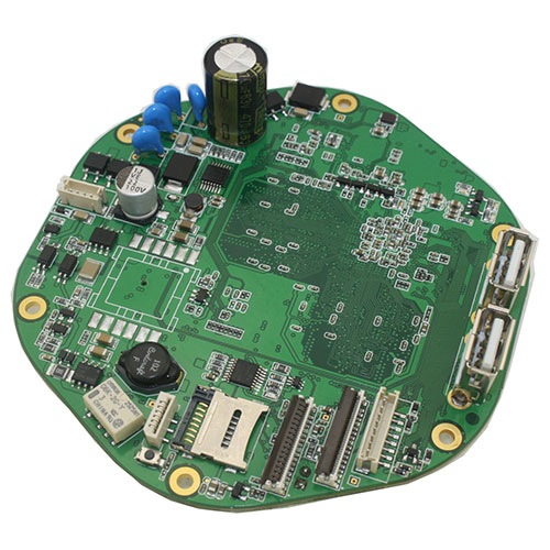
鑫景福致力于滿足“快速服務,零缺陷,輔助研發”PCBA訂購單需求。


PCBA方案設計
Did you not pay attention to the design of pads in PCB design?
When PCB pads are designed in PCB design, they need to be designed in strICt accordance with relevant requirements and standards. Because in SMT chip processing, the design of PCB pad is very important. The pad design will directly affect the solderability, stability and heat transfer of components, as well as the chip processing quality. What is the PCB pad design standard?
1、 PCB pad shape and size design standards:
1. Call PCB standard package library.
2. The minimum single side of the pad shall not be less than 0.25mm, and the maximum diameter of the entire pad shall not be greater than 3 tiMES of the element aperture.
3. Try to ensure that the distance between the edges of two pads is greater than 0.4 mm.
4. Pads with hole diameter more than 1.2mm or pad diameter more than 3.0mm shall be designed as diamond or quincunx pads
5. In case of dense wiring, oval and oblong connecting discs are recommended. The diameter or minimum width of single panel pad is 1.6mm; The hole diameter of the weak current circuit pad of the double-sided board is only required to add 0.5mm, and excessive pad size may cause unnecessary continuous welding.
2、 PCB pad via size standard:
The inner hole of the pad is generally not less than 0.6mm, because it is not easy to process holes SMAller than 0.6mm when punching. Generally, the diameter of the metal pin plus 0.2mm is taken as the inner hole diameter of the pad. For example, when the diameter of the resistance metal pin is 0.5mm, the inner hole diameter of the pad corresponds to 0.7mm, and the diameter of the pad depends on the inner hole diameter.
3、 Key points of PCB pad reliability design:
1. Symmetry: To ensure the balance of the surface tension of molten solder, the pads at both ends must be symmetrical.
2. The space between pads, too large or too small space between pads will cause welding defects, so it is necessary to ensure that the space between component ends or pins and pads is appropriate.
3. The remaining size of the pad, after the component end or pin is lapped with the pad, must ensure that the solder joint can form a meniscus.
4. The width of bonding pad shall be basically consistent with the width of component end or pin.
With correct PCB pad design, if there is a small amount of skew during chip processing, it can be corrected due to the effect of surface tension of molten solder during reflow soldering. If the PCB pad design is not correct, even if the mounting position is very accurate, it is easy to have component position offset, suspension bridge and other welding defects after reflow soldering. Therefore, great attention should be paid to PCB pad design when PCB design is carried out. PCB manufacturers, PCB designers and PCBA manufacturers explain the design of pads in PCB design


抖音二維碼

Q Q二維碼

微信二維碼
點擊
然后
聯系
然后
聯系
電話熱線
13410863085Q Q

微信

- 郵箱