鑫景福致力于滿足“快速服務,零缺陷,輔助研發”PCBA訂購單需求。


PCBA方案設計

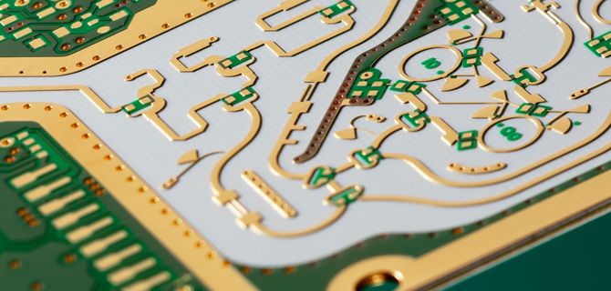
Through Hole design of High Speed PCB
In high speed PCBBoard Design, through-hole design is an important factor, including holes, pad areas around holes and power layer isolation areas, whICh are generally divided into three categories: blind holes, buried through-hole and straight through-hole In the process of PCB design, by analyzing the parasitic capacitance and inductance of the via, some attentions in high-speed PCB via design are summarized Printed circuit board (PCB) is an important supplier of electronIC components, electronic component support and electronic component power connection Because it is made of electronic printing, it is calLED a "printed" circuit board At present, high-speed PCB design is widely used in communication field, computer, graphics and image processing and other fields All high-tech value-added electronic products are designed in pursuit of low power consumption, low electromagnetic radiation, high reliability, miniaturization and lightweight To achieve this goal, via design is an important factor in high-Speed PCB design
PCB board

1. Via
Via is an important factor in multi-layer PCB design. The through hole is mainly composed of three parts, one is the hole; The other is the pad area around the hole; The third is the power layer isolation area The process of through-hole is to coat a layer of metal on the cylindrical surface of the through-hole wall by chEMIcal deposition to connect the copper foil that needs to be connected in the intermediate layer. The upper and lower sides of the through-hole are made of ordinary pads The shape can be directly connected to the upper and lower lines or not connected Through holes can be used for power connection, fixing or positioning equipment The vias are generally divided into three categories: blind vias, embedded vias and through vias Blind hole, located on the top and bottom surfaces of the printed circuit board, with a certain depth, is used to connect the surface circuit and the bottom internal circuit The depth and diameter of the hole usually do not exceed a certain proportion Embedded hole refers to the connection hole located in the inner layer of the printed circuit board, which will not extend to the surface of the circuit board The blind hole and the buried hole are located in the inner layer of the circuit board and are completed by the through hole forming process before lamination In the process of through-hole formation, several inner layers can overlap Through hole, through the entire circuit board, can be used for internal interconnection or as a mounting hole for components Because through-hole is easier to realize in the process and has lower cost, it is usually used in printed circuit boards
2. Parasitic capacitance of vias
The via itself has parasitic capacitance to the ground. If the isolation hole diameter of the through-hole on the ground plane is D2, the diameter of the through-hole pad is D1, the thickness of the PCB is T, and the dielectric constant of the board substrate is Q μ, then the parasitic capacitance of the through-hole is about C=1.41 Q μ TD1/((D2-D1)) The main effect of via parasitic capacitance on the circuit is to prolong the signal rise time and reduce the circuit speed The SMAller the capacitance, the smaller the influence
3. Parasitic inductance of vias
The via itself has parasitic inductance. In the design of high-speed digital circuits, the harm caused by via parasitic inductance is usually greater than that caused by parasitic capacitance Parasitic series inductance of via will weaken the influence of bypass capacitor and reduce the filtering effect of the whole power system If L is the inductance of the through-hole, h is the length of the through-hole, and d is the diameter of the central drilling hole, the parasitic inductance of the through-hole is about L=5.08h [ln (4h/d)+1] It can be seen from the formula that the diameter of the through-hole has little influence on the inductance, while the length of the through-hole will affect the inductance
4. Non-penetrating via technology
Non-through vias include blind vias and buried vias. In non through-hole technology, the application of blind holes and embedded holes can greatly reduce the size and quality of PCB, reduce the number of layers, improve electromagnetic compatibility, add features of electronic products, reduce costs, and also make the design easier and faster There are many problems in traditional PCB design and processing First, they occupy a large amount of effective space. Secondly, a large number of vias are densely distributed in one place, which also brings a huge obstacle to the inner layer wiring of multilayer PCB These vias occupy the space required for wiring, and they pass through the power supply and ground intensively The surface of the conductor layer will also destroy the impedance characteristics of the power ground layer, making the power ground layer invalid The workload of conventional mechanical drilling will be 20 tiMES that of non penetrating drilling technology In PCB design, although the size of pads and vias has gradually decreased, if the thickness of the board layer does not decrease proportionally, the aspect ratio of vias will increase, and the increase of the aspect ratio of vias will reduce the reliability With the maturity of advanced laser drilling technology and plasma dry etching technology, non penetrating small blind holes and small buried holes can be applied If the aperture of these non through-hole holes is 0.3mm, the parasitic parameters they bring are about 1/10 of the original conventional holes, which improves the reliability of PCB Due to the use of non through-hole technology, there are almost no large through-hole on PCB, thus providing more space for traces The remaining space can be used for large area masks to improve EMI/RFI performance At the same time, more remaining space can also be used for the inner layer to partially mask equipment and key network cables, making them power efficient The use of non through-hole makes it easier to fan out device pins. Making high sensitivity pin devices (such as BGA packaged devices) easy to route shortens the connection length and meets the timing requirements of high-speed circuits
5. Via selection in ordinary pcb
In order PCB design, parasitic capacitance and inductance of via have little influence on PCB design For 1-4 layer PCB design, 0.36mm/0.61mm/1.02mm (drilling/pad/POWER isolation area) is generally selected.) vias are better. For some special signal lines (such as power lines, grounding wires, clock lines, etc.), 0.41mm/0.81mm/1. You can select 32mm through holes or other sizes according to the actual situation
6. Via design in high speed PCB
Through the above analysis of the parallel characteristics of vias, we can see this in the design of high-speed PCB. The seemingly SIMple through-hole often brings great negative effects to circuit design You can try to do as much as possible in the design:
(1) Select a reasonable via size. For multilayer PCB design with general density, it is better to use 0.25mm/0.51mm/0.91mm (drilling/pad/POWER isolation area) via; for some high sensitivity PCBs, 0.20mm/0.46mm through-hole/0.86mm, you can also try non through-hole; You can consider using a larger size to reduce the impedance;
(2) The bigger the POWER isolation area, better. Considering the through-hole density on the PCB, generally D1=D2+0.41;
(3) The signal traces on the PCB should not be changed as much as possible, that is, the vias should be minimized;
(4) Using a thinner PCB is conducive to reducing the two parasitic parameters of vias;
(5) The pins of the power supply and the ground should be close to the via hole. The shorter the wires between the through-hole and the pin, the better, because they will add inductance At the same time, the leads of power and ground should be as thick as possible to reduce impact;
(6) Place some ground vias near the vias where the signal changes layers to provide a short-distance loop for the signal.
Of course, the design needs to analyze specific problems in detail Considering the cost and signal quality at the same time, in high-speed PCB design, designers always want the through-hole to be as small as possible, so that more wiring space can be left on the circuit board The parasitic capacitance is also small, which is more suitable for high-speed circuits In the design of high-density PCB, the use of non through-hole and the reduction of via size also bring new costs, and the via size cannot be infinitely reduced It is affected by PCB manufacturers' drilling and electroplating processes Due to the limitation of science and technology, high-speed via design of PCB should be balanced
PCB Design of Digital Analog Mixed Circuit
11-08,2022


抖音二維碼

Q Q二維碼

微信二維碼
點擊
然后
聯系
然后
聯系
電話熱線
13410863085Q Q

微信

- 郵箱