鑫景福致力于滿足“快速服務,零缺陷,輔助研發”PCBA訂購單需求。


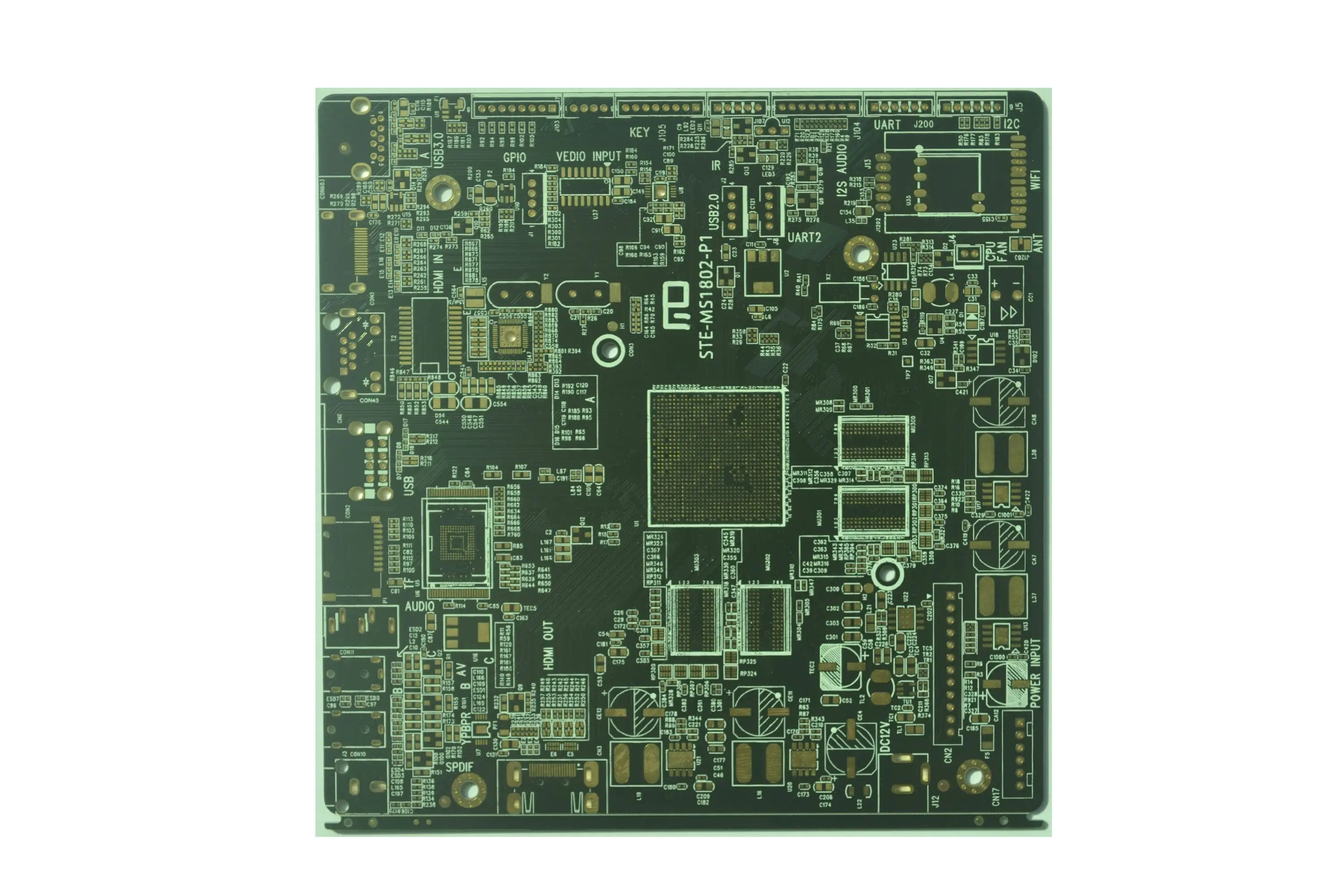
PCBA方案設計

The anti-interference design of printed circuit board
The design quality of PCB proofing PCB not only directly affects the reliability of electronIC products, but also relates to the stability of products, and even is the key to the success of the design. Therefore, when designing and drawing the PCB, in addition to providing correct electrical connection for the components in the circuit, the anti-interference of the PCB should also be fully considered. Based on the principle of electromagnetic compatibility, the anti-interference design should include three aspects: first, to suppress the noise source, second, to cut off the noise transmission path, and third, to reduce the noise sensitivity of the disturbed equipment. The noise suppression of printed boards should start from the design stage and run through a series of links such as circuit schematIC design, printed board drawing design, component selection, and printed board installation leads. Although each link has different emphasis, it echoes each other and should be taken seriously.
This paper mainly introduces how to effectively suppress noise when designing PCB. Reduce radiated noise The printed circuit board will radiate noise outward during operation and become a noise source: the signal wire in the circuit board is transmitted to the chassis through the grounding circuit, causing resonance, and radiates strong noise outward from the chassis; The signal of the circuit board radiates noise outward through the signal cable; The circuit board itself also radiates noise directly. To weaken the noise radiation, the following measures can be taken:
(1) Be careful in selecting devices. Pay attention to the aging problem of components when selecting, and select components with SMAll thermal feedback effect. For high-frequency circuits, appropriate chips shall be selected to reduce circuit radiation. When selecting logic devices, it is necessary to fully consider their noise tolerance indicators: when only considering the noise tolerance of the circuit, it is better to use HTL; if considering power consumption, it is better to use CMOS with VDD ≥ 15V.
(2) Use multilayer printed circuit boards. In this way, the ideal shielding effect can be obtained from the structure: the middle layer is used as the power line or ground wire, the power line is seaLED in the board, and the two sides are insulated, so that the switching currents flowing through the upper and lower layers do not affect each other; The inner layer of the printed circuit board is made into a large conductive area. There is a large electrostatic capacitance between the wire surfaces, forming a power supply circuit with extremely low impedance, which can effectively prevent the circuit board from radiating and receiving noise.
(3) Printed circuit board "fully grounded". When drawing the high-frequency circuit board, in addition to thicken the grounding printed wire as much as possible, all areas not occupied on the circuit board shall be used as grounding wires to make the components better grounded nearby. This can effectively reduce the parasitic inductance, at the same time, a large area of ground wire can effectively reduce noise radiation.
(4) Attach one or both grounding plates to the printed circuit board. Namely, an aluminum sheet or iron sheet is attached to the back of the printed board (welding surface), or the printed board is clamped between two aluminum sheets or iron sheets. The grounding plate shall be installed as close to the printed circuit board as possible, and must be connected to the best grounding point (SG) of the system signal. This structure is essentially a SIMple and easy to do "multilayer" printed circuit board. If you want to pursue a better suppression effect, you can install the printed board in a completely shielded metal box, so that it does not produce or respond to noise.
Properly laying printed wiring is the key stage of graphic design of printed circuit board. Many factors considered in the design should be reflected in the wiring. The layout of copper foil wires on the printed circuit board and the crosstalk between adjacent wires and other factors will determine the immunity of the printed circuit board. Reasonable wiring can make the printed circuit board obtain the best performance. In consideration of anti-interference, the following design and process principles should be followed for wiring:
(1) As long as the wiring requirements are met, single panel shall be preferred, followed by double-sided board and Multilayer board. The wiring density shall be reasonably selected based on the requirements of structure and electrical performance to ensure simple and uniform wiring; The minimum width and spacing of conductors shall not be less than 0.2mm generally. If the wiring density allows, the printed conductors and their spacing shall be widened appropriately.
(2) The main signal lines in the circuit should be gathered in the center of the board as close as possible to the ground wire or surrounded by the ground wire. The area of the loop formed by the signal lines and signal return lines should be the smallest; Long distance parallel wiring shall be avoided as far as possible, and the wiring between electrical interconnection points in the circuit shall be as short as possible; The corner of signal (especially high-frequency signal) line shall be designed as 135 ° trend, or in circular or circular arc shape. It is forbidden to draw 90 ° or smaller angle shape.
(3) The conductors on adjacent wiring surfaces shall be perpendicular, oblique or curved to each other to reduce parasitic coupling; High frequency signal conductors must not be parallel to each other to avoid signal feedback or crosstalk. A ground wire can be added between two parallel lines.
(4) Properly lay the external signal line, shorten the input lead as much as possible, and improve the input terminal impedance. It is better to shield the analog signal input line. When there are analog and digital signals on the board at the same time, the ground wires of both should be isolated to avoid mutual interference.
(5) Properly handle redundant inputs of logic devices. Connect the redundant input terminal of the AND/NAND gate to "1" (never hang in the air), or connect the redundant input terminal of the NAND gate to Vss, and connect the idle set/reset terminals of the counter, register and D trigger to Vcc through appropriate resistance. The redundant input terminal of the trigger must be grounded.
(6) Select standard components for packaging. To create a component package, the pad hole spacing should be consistent with the device pin spacing to reduce lead impedance and parasitic inductance. The metallized through-hole shall be reduced as much as possible when laying wires to improve the reliability of the whole printed board.
PCB manufacturers, PCB designers and PCBA manufacturers will explain the anti-interference design of PCB.


抖音二維碼

Q Q二維碼

微信二維碼
點擊
然后
聯系
然后
聯系
電話熱線
13410863085Q Q

微信

- 郵箱