鑫景福致力于滿足“快速服務,零缺陷,輔助研發”PCBA訂購單需求。


PCBA方案設計
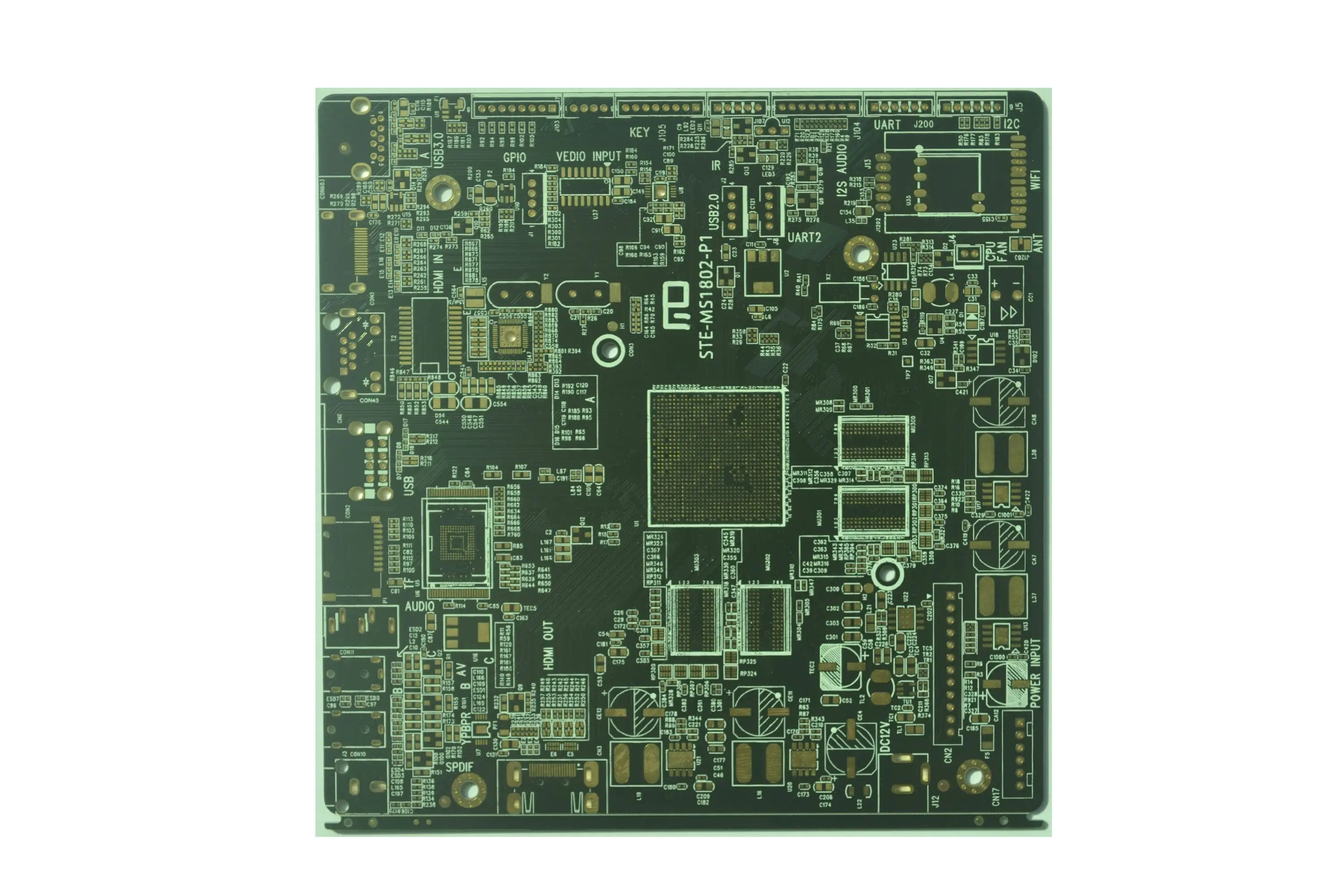
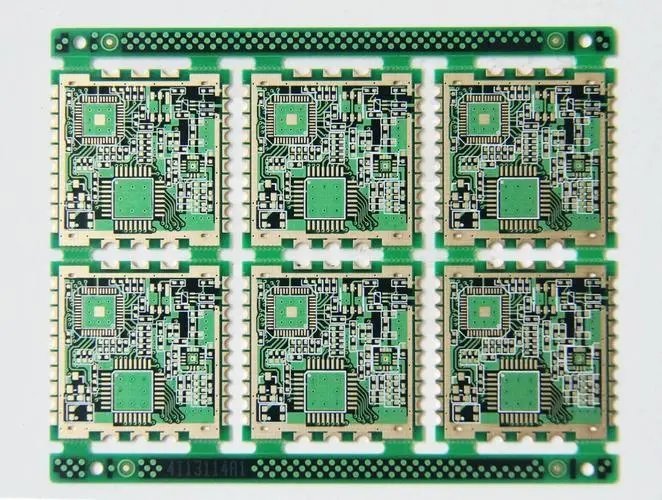
The editor of the electronICs factory explains some principles of pcb wiring
The wiring shall be carried out according to the following principles:
① In general, the power line and ground wire shall be wired first to ensure the electrical performance of the circuit board. Within the allowable range, the width of power supply and ground wire shall be widened as much as possible. It is better to make the ground wire wider than the power line. Their relationship is: ground wire>power line>signal line. Generally, the width of signal line is 0.2~0.3mm, the thinnest width can reach 0.05~0.07mm, and the power line is generally 1.2~2.5mm. The PCB of digital circuit can be used to form a loop with a wide ground wire, that is, to form a ground grid for use (the ground of analog circuit cannot be used in this way)
② Wires with strict requirements (such as high-frequency lines) shall be wired in advance, and the side lines of input and output terminals shall not be adjacent and parallel to avoid reflection interference. If necessary, ground wires shall be added for isolation, and the wiring of two adjacent layers shall be perpendicular to each other, which may cause parasitic coupling.
③ The oscillator shell shall be grounded, and the clock wire shall be as short as possible and shall not be LED everywhere. The area of the ground under the clock oscillation circuit and special high-speed logic circuit should be added, and other signal lines should not be used to make the surrounding electric field approach zero;
④ The 45o polyline wiring shall be used as far as possible, and the 90o polyline shall not be used to reduce the radiation of high-frequency signals; (Double arc lines are also used for lines with high requirements)
⑤ Any signal line shall not form a loop. If it is unavoidable, the loop shall be as SMAll as possible; The vias of signal lines shall be as few as possible;
⑥ The key lines shall be as short and thick as possible, and protective areas shall be added on both sides.
⑦ When transmitting sensitive signals and noise field band signals through flat cables, they should be led out in the way of "ground wire signal ground wire".
⑧ Test points shall be reserved for key signals to facilitate production, maintenance and detection
⑨ After the schematic wiring is completed, the wiring shall be optimized; At the same time, after the preliminary network inspection and DRC inspection are correct, fill the ground wire in the unrouted area, use a large area of copper layer as the ground wire, and connect the unused places with the ground on the printed board as the ground wire. Or it can be made into multilayer boards, with one layer for power supply and one layer for ground wire.
① . Line
In general, the signal line width is 0.3mm (12mil), and the power line width is 0.77mm (30mil) or 1.27mm (50mil); The distance between lines and between lines and pads shall be greater than or equal to 0.33mm (13mil). In practical application, if conditions permit, the distance shall be increased;
When the wiring density is high, it can be considered (but not recommended) to use two lines between IC pins, the width of the line is 0.254mm (10mil), and the line spacing is not less than 0.254mm (10mil). Under special circumstances, when the device pins are dense and the width is narrow, the line width and line spacing can be appropriately reduced.
② . PAD
The basic requirements for PAD and VIA are: the diameter of PAD is greater than that of hole by 0.6 mm; For example, universal pin resistors, capacitors, integrated circuits, etc., adopt 1.6mm/0.8mm (63mil/32mil) disk/hole size, 1.8mm/1.0mm (71mil/39mil) socket, pin, diode 1N4007, etc. In practical application, it shall be determined according to the size of the actual component. If possible, the pad size can be appropriately increased;
The component installation hole diameter designed on the PCB shall be 0.2~0.4mm larger than the actual size of the component pin.
③ . VIA
Generally 1.27mm/0.7mm (50mil/28mil);
When the wiring density is high, the via size can be appropriately reduced, but should not be too small, and 1.0mm/0.6mm (40mil/24mil) can be considered.
④ Requirements for spacing of pads, wires and vias
PAD and VIA : ≥ 0.3mm(12mil)
PAD and PAD : ≥ 0.3mm(12mil)
PAD and TRACK : ≥ 0.3mm(12mil)
TRACK and TRACK : ≥ 0.3mm(12mil)
When the density is high:
PAD and VIA : ≥ 0.254mm(10mil)
PAD and PAD : ≥ 0.254mm(10mil)
PAD and TRACK : ≥ 0.254mm(10mil)
TRACK and TRACK : ≥ 0.254mm(10mil)
Fifth: wiring optimization and silk screen printing. "There is no best, only better"! No matter how hard you try to design, after you finish painting, you will still feel that there are many places that can be modified. The general design experience is that the time for optimal routing is twice as long as the time for initial routing. I don't think there is anything that needs to be modified. After that, I can lay copper (Place ->polygon plane). Copper is generally laid with ground wire (pay attention to the separation of analog ground and digital ground), and power supply may also be required for multi-layer boards. For silk screen, it should be noted that it cannot be blocked by devices or removed by vias and pads. At the same time, when designing, face up to the component surface, and the characters at the bottom layer should be mirrored to avoid confusing the layers.
Sixth: Network and DRC inspection and structure inspection. First, on the prEMIse of confirming that the circuit schematIC design is correct, NETCHECK the generated PCB network file and the schematic network file for the physical connection relationship, and correct the design in time according to the output file results to ensure the correctness of the wiring connection relationship;
After the network check is passed correctly, DRC check shall be carried out on the PCB design, and the design shall be corrected in time according to the output file results to ensure the electrical performance of PCB wiring. Finally, it is necessary to further check and confirm the mechanical installation structure of PCB.
Seventh: Plate making. Before that, it is better to have an audit process.
PCB design is a mental work. The Board Designed by the person who is thoughtful and experienced is good. Therefore, we should be extremely careful in design, fully consider all factors (for example, many people do not consider the convenience of maintenance and inspection), and strive for perfection, so that we can design a good board.
PCB manufacturers, PCB designers and PCBA manufacturers explain some principles of PCB wiring.


抖音二維碼

Q Q二維碼

微信二維碼
點擊
然后
聯系
然后
聯系
電話熱線
13410863085Q Q

微信

- 郵箱