鑫景福致力于滿足“快速服務,零缺陷,輔助研發”PCBA訂購單需求。


PCBA方案設計
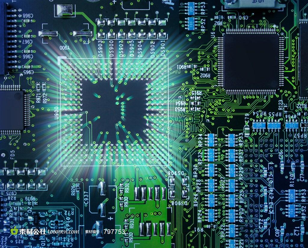
Techniques for Reducing RF Effects in PCB Interconnection Design
This paper will introduce various technologies for designing three kinds of interconnects between chips and boards, internal interconnection PCB boards, as well as PCB and external equipment, including equipment installation, wiring isolation, and measures to reduce lead inductance, Help designers reduce RF effect in PCB board interconnection design The interconnection of circuit board system includes: chip to circuit board, internal interconnection PCB, and three types of interconnection PCB and external equipment In RF design, the electromagnetIC characteristic of interconnection point is one of the main problems in engineering design This paper introduces various technologies of the above three interconnection designs, including equipment installation methods, wiring isolation, and measures to reduce lead inductance At present, there are indications that the frequency of PCB design is getting higher and higher With the increasing data rate, the bandwidth required for data transmission also pushes the upper limit of signal frequency to 1 GHz or higher This high frequency signal technology, while well beyond mmWave technology (3.0GHz), also involves RF and low-end microwave technology RF engineering methods must be able to deal with stronger electromagnetic field effects that usually occur at higher frequencies These electromagnetic fields can be traced on adjacent signal lines or PCB boards, causing unwanted cross talk (interference and total noise) and affecting system performance Return loss is mainly caused by impedance miSMAtch, which has the same effect on signal as additional noise and interference
PCB board

High return losses have two negative effects:
1) The reflection of the signal back to the signal source will increase the system noise, making it more difficult for the receiver to distinguish the noise from the signal;
2) Any reflected signal basically degrades the signal quality because the shape of the input signal changes.
Although digital systems are very fault-tolerant, because they only deal with 1 and 0, the harmonics generated when high-speed pulses rise will result in weak signals at higher frequencies Although forward error correction technology can eliminate some negative effects, some system bandwidths are used to transmit redundant data, resulting in reduced system performance A better solution would be for RF effects to contribute to signal integrity rather than reduce it The recommended total return loss at digital system frequencies (usually point data points) is - 25dB, which is equivalent to the design of a target PCB with a VSWR of 1.1 For RFPCB boards, high-speed signals sometiMES limit PCB design At present, the main solutions to the crosstalk problem are ground level management, track spacing and reducing lead inductance The main method to reduce return loss is impedance matching The method includes effective management of insulating materials and isolation of source signal line and ground wire, especially between signal line and ground where state transition occurs Because the interconnection point is the weak link in the circuit chain, the electromagnetic characteristics of the interconnection point is the main problem faced by the engineering design in the RF design. Each interconnection point should be checked and the existing problems should be solved The interconnection of circuit board system includes three types of interconnection, such as chip to circuit board, interconnection in PCB, and output between signal input/PCB and external equipment
1. Chips and PCB boards
Pentium IV and high-speed chip/output interconnect points with a large number of inputs are available As far as the chip itself is concerned, its performance is reliable and the processing speed has reached 1GHz The excitement of the near GHz interconnection sEMInar: how to deal with the growing I/O system is well known The main problem of chip to PCB interconnection is that the interconnection density is too high, which leads to the basic structure of PCB data becoming the limiting factor of interconnection density growth
2. Interconnection in the PCB
The skills and methods for high frequency PCB design are as follows:
2.1 The corner of the transmission line should be 45° to reduce the return loss;
2.2 High performance insulated circuit board shall be adopted, and the insulation rating shall be controlLED strictly according to the grade This method helps to effectively manage the electromagnetic field between insulating materials and adjacent wiring
2.3 It is necessary to improve the design specification for high-precision etching of PCB Considering that the specified total error is++/- 0. The line width is 0007 inches, manage the undercut and cross section of the wire shape, and specify the plating conditions of the wiring sidewall Overall management of wiring (conductor) geometry and coating surfaces is important to address skin effect issues associated with microwave frequencies and to achieve these specifications.
2.4 There is a tap inductance on the protruding wire. Please note this and avoid using leaded parts For high frequency environment, use surface mount components
2.5 Used for signal vias, avoid using the via processing (pth) process on sensitive boards because this process will cause lead induction at the via For example, when the via on the 20 layer board is used to connect layers 1 to 3, the lead inductance will affect layers 4 to 19
2.6 Provide rich ground surface Molded vias are used to connect these ground planes to prevent the effects of 3D electromagnetic fields on the circuit board
2.7 Select electroless nickel plating or immersion gold plating process, and do not use HASL method for electroplating This electroplating surface provides better skin effect for high-frequency current In addition, this highly solderable coating requires fewer wires to help reduce environmental pollution
2.8 Solder resist film prevents solder paste from flowing However, due to the uncertainty of thickness and unknown insulation characteristics, covering the entire circuit board surface with solder mask data will lead to huge changes in electromagnetic energy in microstrip design The weld stop is usually used as a solder mask
If you are not familiar with these methods, consult an experienced military microwave circuit board design engineer You can also discuss with them the price range you can afford For example, coplanar microstrip design with copper on the back is more economical than stripline design. You can discuss this with them for better advice Engineers may not be used to thinking about costs, but their advice can be very helpful It will be a long-term effort to try to train young engineers who are unfamiliar with radio frequency effects and lack experience in dealing with them In addition, other solutions are available, such as retrofitting computers to handle RF effects
3. Interconnecting PCB boards and external devices between
It can now be considered that we have solved all the signal management issues on the board and on the interconnection of the various discrete components. So how to solve the signal input/output problem from the circuit board to the wire connected to the remote device? In this case, we manage the transition between microstrip and coaxial cable In coaxial cable, the ground plane is interlaced into a ring with uniform spacing In the microstrip, the horizon is below the active line This introduces some edge effects that need to be understood and predicted and considered in the design Of course, this mismatch will also lead to loss of returns, and noise and signal interference must be reduced The management of impedance problem in circuit board is not a design problem that can be ignored Impedance starts at the surface of the circuit board, passes through solder joints to the connector, and ends at the coaxial cable Because impedance varies with frequency, the higher the frequency, the more difficult impedance management becomes The problem of using higher frequency to upload and transmit signals in broadband seems to be PCB design

Overview of PCB Failure Analysis Technology
11-09,2022


抖音二維碼

Q Q二維碼

微信二維碼
點擊
然后
聯系
然后
聯系
電話熱線
13410863085Q Q

微信

- 郵箱