鑫景福致力于滿足“快速服務(wù),零缺陷,輔助研發(fā)”P(pán)CBA訂購(gòu)單需求。


PCBA方案設(shè)計(jì)

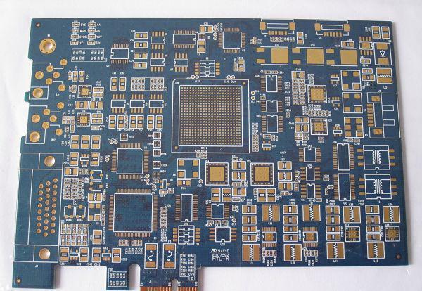
PCB design: solve problems, reduce costs and improve effICiency
Many problems need to be considered in the design process. PCB and tools, including DesignSpark PCB, can effectively handle most problems By using some practical guidelines, engineers can effectively reduce costs, improve the reliability of circuit boards, and at the same time meet the system specifications, so as to transfer the system at a lower cost and avoid more problems Design of printed circuit board refers to the circuit layout through the design of schematic diagram and the production of printed circuit board at the lowest possible cost In the past, this was usually done with the help of expensive special tools, but now, the increasing availability of high-performance software tools (such as DesignSpark PCB and design model) has greatly accelerated the design speed of circuit board designers Although engineers know that perfect design is the way to avoid problems, it is still a waste of time and money, while solving the symptoms rather than the root cause For example, if a problem is discovered during the electromagnetic compatibility (EMC) testing phase, which will lead to a lot of cost investment, even the original design needs to be adjusted and reworked, which takes several months
printed circuit board

Layout is one of the most important problems faced by designers This problem depends on each part of the drawing, and some devices need to be combined according to logical considerations It should be noted, however, that temperature sensing elements, such as sensors, should be placed separately from heating components, including power converters For designs with multiple power settings, 12V and 15V power converters can be placed at different positions on the circuit board because the thermal noise and electrical noise generated by them will affect the reliability and efficiency of other components and the circuit board. The above components will also affect the electromagnetic efficiency of the circuit design, which is very important not only for the efficiency and energy consumption of the circuit board, but also for the economy of the circuit board, All circuit board equipment sold in Europe must be CE MARKed to prove that they will not interfere with other systems However, this usually only coMES from the power side, and many other devices will make noise, such as DC-DC converters and high-speed data converters Due to the imperfect design of the circuit board, this noise can be captured by the channel and radiated as a SMAll antenna, generating spurious noise and abnormal frequency Far-field electromagnetic interference (EMI) problems can be solved by adding filters at the noise point or shielding the signal with a metal enclosure. However, paying enough attention to the equipment that can emit electromagnetic interference (EMI) on the circuit board allows the circuit board to choose a cheaper casing effectively reduces the cost of the whole system
Electromagnetic interaction (EMI) is inserted a factor that has to be taken into account in the design process of PCB electromagnetic crosstalk can couple with the channel, which can scramble the signal into noise and affect the overall efficiency of the circuit board If the coupling noise is too high, the signal may be completely covered. In retrOSPect, a more expensive signal amplifier must be instalLED to restore it to normal However, if the signal line layout can be fully considered when designing the circuit board, the above problems can be avoided Because the design of the circuit board will vary according to different equipment, different places of use, different heat dissipation requirements, and different electrical interface (EMI) conditions, at this time, the design template will be useful Capacitance is also an important problem in circuit board design, because it affects signal propagation speed and adds power consumption Channels can be coupled to adjacent traces or run vertically through two circuit layers to inadvertently form capacitors This problem can be solved relatively easily by reducing the length of parallel lines, adding kinks to one of the lines to break the coupling, etc However, this also requires engineers to fully consider the production design principles to ensure that the design is easy to manufacture and avoid any noise radiation caused by excessive bending angle of the line The distance between lines may also be too close, which will form a short circuit between lines, especially at the bend of lines. As time goes on, metal "whiskers" will appear The design rule check can usually mark areas where the loop risk is higher than normal This problem is particularly prominent in ground plan design A metal circuit layer that may be coupled to all tracks above and below it Although the metal layer can effectively block noise, the metal layer also generates related capacitance, which will affect the operating speed of the circuit and increase power consumption As far as the design of multilayer circuit boards is concerned, the design of vias between different layers of circuit boards may be a controversial issue, because the design of vias will bring many problems to the production and manufacturing of circuit boards The through-hole between circuit board layers will affect the signal efficiency and reduce the reliability of circuit Board Design
Solution: In the design process, many different methods can be adopted to solve various problems of PCB it includes the adjustment of the design scheme itself, such as adjusting the circuit layout to reduce noise; There are also some methods for PCB layout design components can be automatically installed through the layout tool, but the ability to manually adjust the automatic layout will help improve the quality of circuit board design Through this measure, the design rule check will rely on the scientific and technological archives to ensure that the design of the circuit board meets the requirements of the Circuit board manufacturer Separating different circuit board layers can reduce the associated capacitance. However, this increases the number of layers on the circuit board, which increases the cost and brings more through-hole problems Although the use of orthogonal grid power system and grounding trajectory design may increase the physical size of the circuit board, it can effectively use the grounding layer in the two-layer circuit board to reduce the complexity of capacitance and circuit board manufacturing Design tools, including DesignSpark PCB, can help engineers solve many problems at the beginning of design, but engineers still need to have a good understanding of PCB For example, if the editing of a printed circuit board needs to know the number of layers of the circuit board at the beginning of design, for example, a double-layer circuit board needs to have a grounding layer and a power layer, which are composed of independent layers
It is very useful to use automatic component placement technology, which can help designers spend more time designing the layout area of the equipment For example, if the power supply is too close to sensitive signal lines or high temperature areas, many problems will occur With the same conduit, the signal line can also be automatically routed to avoid most problems. However, the analysis and manual operation of high-risk areas will help greatly improve the quality and profitability of PCB design and reduce the overall cost Design rule checking is also a very powerful tool for checking lines to ensure that the distance between lines is not too close, resulting in too short loops However, the overall design still has high economic value The design planning inspection tool can also be used to check and adjust the power supply and ground plane to avoid excessive parasitic capacitance area The above tools are also very helpful for Gerber and Excelon in wiring and PCB, as well as through hole drilling, in order to produce the final design With this kind of pipeline, scientific and technological archives are closely related to circuit board manufacturers
In the process of PCB design, there are many problems to consider, and tools, including DesignSpark PCB, can effectively handle most problems By using some practical guidelines, engineers can effectively reduce the cost, improve the reliability of the circuit board, and at the same time meet the system specifications, transfer the system at a lower cost, and avoid more problems with the printed circuit board


抖音二維碼

Q Q二維碼

微信二維碼
點(diǎn)擊
然后
聯(lián)系
然后
聯(lián)系
電話熱線
13410863085Q Q

微信

- 郵箱