鑫景福致力于滿足“快速服務,零缺陷,輔助研發”PCBA訂購單需求。


PCBA方案設計
Talking about the Manufacture of PCB from Five Aspects
Everyone knows that a PCB is a PCB that turns a designed schematIC into a reality Please do not underestimate this process There are many things that are feasible in principle, but difficult to achieve in the project, or things that others can achieve, but others cannot Therefore, it is not easy to make a PCB Two major difficulties in the field of microelectronics are the processing of high frequency signals and weak signals In this regard, the level of PCB production is particularly important The same principle design, the same components, and the S produced by different people with different PCB boards have different characteristics As a result, how can we make PCB?
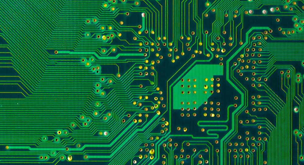
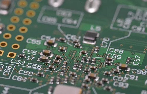
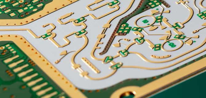
PCB board

1. To clarify the design goals
When receiving a design task, first of all, it is necessary to define the design goal, whether it is an ordinary pcb, a high-frequency PCB, a SMAll signal processing PCB, or whether the PCB has high-frequency and small signal processing For ordinary PCB boards, as long as the layout and wiring are reasonable and neat, and the mechanical dimensions are accurate, if there are medium load lines and long-distance transmission lines, some methods must be used to reduce the load When the signal lines on the circuit board exceed 40MHz, special consideration shall be given to these signal lines, such as crosstalk between lines If the frequency is higher, the wiring length will be more restricted According to the distributed parameter network theory, the interaction between high-speed circuits and their routing is a decisive factor, which cannot be ignored in system design As the transmission rate of the gate increases, the resistance on the signal line will increase correspondingly, and the crosstalk between adjacent signal lines will increase proportionally Generally, the power consumption and heat dissipation of high-speed circuits are also large When manufacturing high-speed PCB, pay full attention to the circuit board When there are millivolt or even microvolt level weak signals on the circuit board, pay special attention to these signal lines Because the small signal is too weak, it is easy to be interfered by other strong signals, and shielding measures are usually required The signal-to-noise ratio is greatly reduced Therefore, useful signals are submerged by noise and cannot be effectively selected The debugging of the circuit board shall also be considered in the design phase The physical location of the test point, the isolation of the test point and other factors cannot be ignored, because some small signals and high-frequency signals cannot be directly added to the probe for measurement In addition, other relevant factors should be considered, such as the number of layers of the circuit board, the packaging shape of the components used, and the mechanical strength of the board In PCB, it is necessary to understand the design objectives
2. Underst and function of the components used for the layout and wiring requirements
We know that some special components have special requirements for layout and wiring, such as analog signal amplifiers used in LOTI and APH Analog signal amplifier needs stable power supply and small ripple The analog small signal part shall be as far away from the power supply equipment as possible On the OTI board, the small signal amplification part is also professionally equipped with a mask cover to mask stray electromagnetic interference The GLINK chip used on the NTOI board uses the ECL process, which consuMES a lot of power and generates heat Special consideration must be given to heat dissipation during layout If natural heat dissipation is used, the GLINK chip must be placed at a place where the air circulation is relatively stable, And heat dissipation will not have a great impact on other chips If the circuit board is equipped with speakers or other high-power equipment, it may cause serious pollution to the power supply, which should also be paid enough attention
3. Consideration of component layout
One of the first factors to be considered in the Layout of components is the electrical performance. Components closely related to the wiring shall be put together as much as possible In particular, the layout of some high-speed lines should be as short as possible Power signal and small signal equipment are separated On the prEMIse of meeting the circuit efficiency, it must also take into account that the components are placed neatly and beautifully for easy testing It is also necessary to carefully consider the mechanical size of the circuit board and the location of the socket The grounding and propagation delay time of interconnects in high-speed systems are also the primary considerations in system design The transmission time on the signal line has a great influence on the speed of the whole system, especially on the high-speed ECL circuit Although the speed of the integrated circuit block itself is very high, due to the use of ordinal interconnecting lines on the backplane (about 30 cm in length per line) 2ns delay) will increase the delay time, which can greatly reduce the system speed Synchronous working parts (such as displacement registers and synchronous counters) are placed on the same workpiece board. Because the transmission delay time of clock signals to different workpiece boards is not equal, this may lead to the main error of the displacement registers Board, where synchronization is critical, the clock lines from the common clock source to each board must be the same length
4. The consideration of wiring
With the completion of the design of OTNI and star fiber network, more circuit boards with high-speed signal lines above 100MHz will be designed in the future Here we will introduce some basic concepts of high-speed lines
4.1 Transmission line
Any "long" signal path on a printed circuit board can be considered a transmission line. If the propagation delay time of the line is far less than the signal rise time, any reflection generated during the signal rise will be submerged Over, rebates and ringtones no longer exist For most current MOS circuits, because the ratio of rise time to line transmission delay time is much larger, the trajectory can be measured in meters without signal distortion Used for faster logic circuits, especially ultrahigh speed ECL For integrated circuits, due to the increase of edge speed, if no other measures are taken, the length of traces must be greatly shortened in order to maintain signal integrity There are two ways to make high-speed circuits work on relatively long lines without serious waveform distortion TTL uses Schottky diode clamp bits to achieve fast falling edge. In this case, the overshoot is clamped as a diode voltage drop lower than the ground potential This reduces the range of subsequent rebates, and the slow rising edge allows overshoot, but it is attended by the relatively high output impact (50-80 °) ?) Of the circuit in the level "H" state. In addition, due to the high immunity of the "H" state, the recoil problem is not very prominent For HCT series equipment, if Schottky diode clamp and series resistor termination methods are used, the improvement will be improved The effect will be more obvious With higher bit rate and faster edge rate, when there is fan out along the signal line, the above TTL shaping method has some shortcomings Because of the reflected waves in the line, they will tend to combine at high bit rate, causing serious signal distortion and reducing the anti-interference ability Therefore, in order to solve the reflection problem, another method is usually used in ECL system: line impedance matching method This controls reflection and ensures signal integrity Strictly speaking, transmission lines are not necessary for traditional TTL and CMOS devices with slow edge speed Transmission lines are not always required for high-speed ECL devices with faster edge speeds However, when using transmission lines, their advantages are that they can predict wire delay and control reflection and oscillation through impedance matching
4.2 There are five basic factors to decide whether to use the transmission line They are:
(1) The edge rate of the system signal;
(2) Connection distance;
(3) Capacitive load (how much fan-out);
(4) Resistive load (wire termination method);
(5) Permissible recoil and overshoot percentage (reduction in AC immunity).
4.3 Several types of transmission lines
(1) Coaxial cable and twisted pair: They are often used in the connection between systems. The characteristic impedance of coaxial cable is usually 50 ? ? And 75 ? ?, Twisted pair is usually 110 Ω)
(2) Microstrip line on the printed board: The microstrip line is a strip conductor (signal line). Use dielectric to isolate from the ground plane If the distance between the thickness, width and the line ground plane is controllable, the characteristic impedance is also controllable The propagation delay time per tissue length of the microstrip line depends only on the dielectric constant and is independent of the line width or spacing
(3) Stripline in printed boards: A stripline is a copper stripline placed in the middle of a dielectric between two conductive planes. If the thickness and width of the line, the dielectric constant of the medium, and the distance between two conductive planes are controllable, then the characteristic impedance of the line is also controllable SIMilarly, the propagation delay time of each tissue length of the stripline is independent of the line width or spacing; It only depends on the relative permittivity of the medium used
5. PCB wiring technology
Which to choose a double sided or a multilayered board when making a PCB depends on operating frequency, complexity of circuit system and assembly density requirements When the clock frequency exceeds 200MHZ, select Multilayer board If the operating frequency exceeds 350MHz, the printed circuit board with PTFE as the dielectric layer is selected because of its small high-frequency attenuation, small parasitic capacitance and faster transmission speed The following principles are required for the wiring of the printed circuit board
(1) There should be as much space as possible between all parallel signal lines to reduce crosstalk. If there are two signal lines close to each other and the ground wire is connected between the two lines, it can act as a shield
(2) When designing the signal transmission line, sharp turns must be avoided to prevent reflection caused by sudden changes in the characteristic impedance of the transmission line, and try to design it as a uniform arc with a certain size


抖音二維碼

Q Q二維碼

微信二維碼
點擊
然后
聯系
然后
聯系
電話熱線
13410863085Q Q

微信

- 郵箱