鑫景福致力于滿足“快速服務(wù),零缺陷,輔助研發(fā)”PCBA訂購單需求。


PCBA方案設(shè)計(jì)
EMI Control Technology in Digital Circuit PCB Design
1. EM generation and suppression principle
EMI in PCB design is caused by electromagnetIC interference source, which transmits energy to sensitive system through coupling path It includes three basic forms: conductor conduction or common grounding, space radiation, or near-field coupling The hazards of electromagnetic interference are shown as reducing the quality of transmitted signals, causing interference or even damage to circuits or equipment, and making the equipment unable to meet the technical index requirements specified in the electromagnetic compatibility standards
In order to suppress electromagnetic interference, the electromagnetic interference design of digital circuits should be carried out according to the following principles:
1.1 According to relevant EMC/EMI technical specifications, the quota is divided into single board circuits for hierarchical control
1.2. Control of the three elements of electromagnetic interference, namely, interference source, energy coupling path and sensitive system, so that the circuit has a flat frequency response and ensures the normal and stable operation of the circuit
1.3 Start from the front-end design of equipment, pay attention to EMC/EMI design, and reduce the design cost
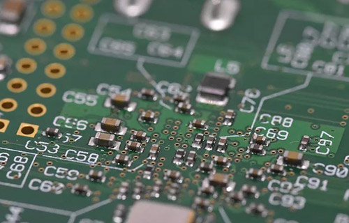
Printed circuit board

2. Digital circuit EMI control technology PCB board
When dealing with various forms of electromagnetic interference, specific problems must be analyzed In PCB digital circuit design, EMI control can be carried out from the following aspects
2.1 Device Selection
In EMI design, the speed of the selected equipment should be considered first Replacing equipment with a rise time of 5ns with any circuit of equipment with a rise time of 2ns. 5ns will increase electromagnetic interference by about 4 tiMES The radiation intensity of electromagnetic interference is proportional to the square of frequency, also known as EMI transmission bandwidth, which is a function of signal rise time rather than signal frequency: fknit=0.35/Tr (where Tr is the signal rise time of the device) The frequency range of this radiated EMI is 30MHz to several GHz. In this frequency band, the wavelength is very short, and even the very short wiring on the circuit board can become a transmitting antenna When EMI is high, the circuit is easy to lose its normal function Therefore, in terms of equipment selection, on the premise of ensuring circuit efficiency requirements, low-speed chips should be used as far as possible, and appropriate driving/receiving circuits should be used In addition, because the lead pin of the device has parasitic inductance and parasitic capacitance, in high-speed design, the influence of device packaging form on the signal cannot be ignored, because it is also an important factor to generate electromagnetic interference radiation In general, the parasitic parameters of SMD devices are SMAller than those of plug-in devices, and the parasitic parameters of BGA packages are smaller than those of QFP packages
2.2 Connector selection and signal terminal definition
Connector is the key link of high speed signal transmission In the terminal design of the connector, more grounding pins can be arranged to reduce the distance between the signal and the ground, reduce the effective signal loop area that generates radiation in the connector, and provide a low impedance return path If necessary, consider isolating some critical signals with ground pins
2.3 Laminate Design
If the cost permits, increase the number of ground plane and place the signal layer next to the ground plane to reduce EMI radiation For high-speed PCB boards, the power supply and ground plane are tightly coupLED to reduce the power supply impedance and thus reduce electromagnetic interference
2.4 Layout
According to the signal current flow, reasonable layout can reduce the interference between signals Correct layout is the key to control electromagnetic interference The basic principles of layout are:
(1) The analog signal is easily interfered by the digital signal, and the analog circuit should be separated from the digital circuit;
(2) The clock line is the main source of interference and radiation, so keep it away from sensitive circuits and keep the clock line short;
(3) Circuits with high current and high power consumption should be avoided as far as possible in the central area of the board, and the influence of heat dissipation and radiation should be considered at the same time;
(4) The connectors should be arranged on one side of the board as far as possible and away from high-frequency circuits;
(5) The input/output circuit is close to the corresponding connector, and the decoupling capacitor is close to the corresponding power pin;
(6) Fully consider the feasibility of layout for power splitting, and multi power devices should be placed across the boundary of power splitting area to effectively reduce the impact of plane splitting on EMI;
(7) The reflow plane (path) is not divided.
2.5 Wiring
(1) Impedance control: High speed signal lines will exhibit the characteristics of transmission lines
(2) Classify the signals, according to the EMI radiation intensity and sensitivity of different signals (analysis signal, clock signal, I/O signal, bus, power supply, etc.), and try to separate the interference source from the sensitive system to reduce coupling
(3) Strictly control the trace length, via number, cross partition, termination, routing layer, return path, etc of clock signals (especially high-speed clock signals).
(4) The signal loop, that is, the loop formed from signal outflow to signal inflow, is the key to EMI control in PCB design and must be controlled during wiring Understand the flow direction of each key signal, and arrange the key signal near the return path to ensure its loop area For low-frequency signals, the path that allows current to flow through the resistor; For high-frequency signals, the path that causes high-frequency current to flow through the inductor is not the path of the resistor The EMI radiation intensity (E) is significant to the current, the area of current loop and the square of frequency (where I is the current, A is the loop area, f is the frequency, r is the distance to the center of the loop, and k is a constant.) So when the inductor return path is just below the signal conductor, the area of the current loop can be reduced, thereby reducing the EMI radiation energy Key signals shall not pass through the segmented area The high-speed differential signal track shall be closely coupled as far as possible Ensure that the stripline, microstrip line and their datum meet the requirements The lead of decoupling capacitor shall be short and wide All signal traces shall be as far away from the edge of the circuit board as possible For a multipoint connection network, select an appropriate topology to reduce signal reflection and EMI transmission
2.6 Split Processing of Power Plane
(1) Division of the power supply layer
When there are one or more sub power supplies on a main power supply plane, ensure the continuity of each power supply area and sufficient copper foil width The dividing line need not be too wide. Generally, the line width of 20-50 mils is enough to reduce gap radiation
(2) Division of the ground layer
The ground plane layer should remain intact to avoid fragmentation. If it is necessary to separate, distinguish digital ground, analog ground and noise ground, and connect them to external ground through the common ground point at the outlet In order to reduce the edge radiation of the power supply, the power/ground plane should follow the 20H design principle, that is, the size of the ground plane is 20H larger than the size of the power plane, reducing the edge field radiation intensity by 70%
3. Other control methods for EMI
3.1 Power System Design
(1) Design a low impedance power system to ensure that the impedance of the power distribution system in the frequency range below fknee is lower than the target impedance.
(2) Use a filter to control conducted interference.
(3) Power supply decoupling. In EMI design, reasonable decoupling capacitor can make the chip work reliably, reduce high-frequency noise in the power supply, and reduce electromagnetic interference Due to the influence of wire inductance and other parasitic parameters, the power supply and its power line respond slowly, which will lead to insufficient transient current required by the driver in high-speed circuit By properly designing bypass or decoupling capacitors and distributed capacitors in the power layer, the energy storage effect of capacitors can be used to quickly supply current to equipment before the power response Proper capacitive decoupling provides a low impedance power path, which is the key to reduce common mode EMI
3.2 Grounding
Grounding design is the key to reducing the EMI of the whole board.
(1) Make sure to use single point grounding
(2) Separate digital ground, analogy grounding and noise grounding, and determine the appropriate public grounding point
(3) If there is no ground wire layer in the double sided design, it is very important to reasonably design the grounding grid Large area paving method can also be used, but it should be noted that the continuity of large area ground on the same layer is better
(4) For the Multi layer board design, ensure that there is a ground plane to reduce the common ground impedance


抖音二維碼

Q Q二維碼

微信二維碼
點(diǎn)擊
然后
聯(lián)系
然后
聯(lián)系
電話熱線
13410863085Q Q

微信

- 郵箱