鑫景福致力于滿足“快速服務(wù),零缺陷,輔助研發(fā)”PCBA訂購(gòu)單需求。


PCBA方案設(shè)計(jì)
Prevention and leveling method of PCB warping
Industry insiders are very aware of PCB warping If SMT electronIC components cannot be instalLED, or the electronIC components (including integrated blocks) have point contact with the solver joints of the printed circuit board, or some feet cannot be cut or cut onto the substrate when installing electronic components; In some parts of the substrate, the pad cannot contact the welding surface, nor can it be welded, etc; One aspect of the cause of warpage of the printed circuit board is that the abstract (copper clad laminate) used may be warped Therefore, the first thing for PCB manufacturers is to prevent PCB from warping during processing; The second is to have a proper and effective method to deal with warpage
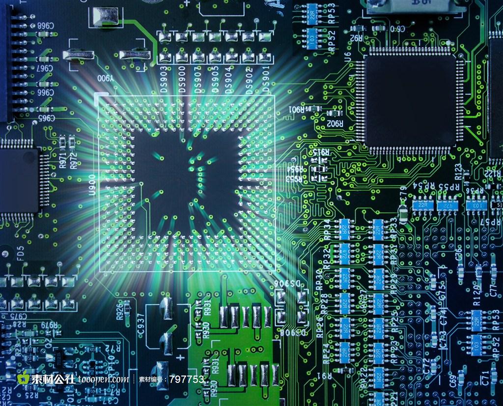
PCB board

1. Prevent the printed circuit board from warping during processing
1.1 Prevent or increase substrate warpage due to improper inventory methods
(1) Due to the vibration absorption of the CCL during the storage process, the warpage will increase, and the moisture absorption area of single-sided CCL is large If the storage environment humidity is high, the single-sided copper clad laminate will significantly increase warpage The moisture of double-sided copper clad laminate can only penetrate from the end face of the product, with SMAll moisture absorption area and slow warping change Therefore, for the copper clad laminate without moisture-proof packaging, pay attention to the warehouse conditions, minimize the humidity in the warehouse, and avoid bare copper clad laminate, so as to avoid new warpage of copper clad laminate during storage
(2) Improper placement of CCL will increase warpage. For example, vertical placement or heavy objects on CCL, poor location, etc, Warpage and deformation of CCL will be added
Welding PCBA
1.2. Avoid warping caused by improper circuit design or improper PCB processing technology
For example, in the conductive circuit diagram of, the PCB board is unbalanced or obviously asymmetrical, and there is a large area of copper sheet on one side, which will form a great pressure and cause the PCB board to twist, and the processing temperature in the PCB process is high or the thermal effect is large, etc This will cause the PCB board to twist For the impact of improper panel inventory method, PCB factories had better solve this problem This is enough to improve the storage environment, prevent vertical placement, and avoid heavy pressure For large area of copper in PCB circuit diagram, copper foil is MEShed to reduce stress
1.3 Eliminate substrate stress and reduce PCB warpage during processing
Because in the process of PCB processing For example, after etching, the substrate needs to be cleaned with water, and it needs to be dried before it can be heated When patterns are plated, the plating is very hot After printing green oil and logo characters, they should be dried by heating or ultraviolet light It's also very big and so on These processes may distort the PCBs
1.4 During wave soldering or DIP soldering, the solder temperature is too high and the operation time is too long, which will also increase the warpage of the substrate For the improvement of wave soldering process, electronic assembly plants need to cooperate
Since stress is the main cause of substrate warping, if the CCL is put into use, the board (also called baked board) is first baked Many PCB manufacturers believe that this method can help reduce PCB boards The function of the baking board is to fully relax the stress of the substrate, so as to reduce the warpage and deformation of the substrate during PCB manufacturing The method of baking circuit boards is: conditional PCB factories use large ovens to bake circuit boards Before putting into production, a large stack of copper clad laminate is sent into the oven, and the copper clad laminate is baked for several hours to 10 hours at a temperature close to the glass transition temperature of the substrate The warpage deformation PCB produced by baking copper clad laminate is relatively small, and the product qualification rate is higher For some small PCB factories, if there is no such large oven, the substrate can be cut into small pieces and baked. However, when baking the plate, there should be a weight to press the plate, so that the substrate can remain flat during stress relaxation The temperature of the baking tray should not be too high. If the temperature is too high, the substrate will change color It should not be too low, because if the temperature is too low, it will take a long time to relax the stress of the substrate
2. Warpage and leveling method of printed circuit board
2.1 Flatten twisted board in time during the PCB manufacturing process
In the PCB manufacturing process, pick out and level the large warped plates with a roller leveler, and then enter the next process Many PCB manufacturers believe that this method can effectively reduce the warpage of finished PCB
2.2 Warpage and leveling method of PCB finished board
For PCB board has been completed, warpage obviously exceeds the tolerance, and cannot be leveled with roller leveler, some PCB factories put it into a small press (or SIMilar fixture) to press the warmed PCB board After several to ten hours of cold pressing and leveling, the effect of this method is not very obvious in practical application First, the leveling effect is not very good, and other is that the flattened board is easy to launch back (that is, to recover warpage) Other PCB manufacturers heat the small press to a certain temperature, then hot press and level the warped PCB The effect is better than cold pressing, but if the pressure is too high, the wire will be deformed; There are defects such as rosin discoloration, substrate discoloration, etc It takes a long time (vertical hours to more than ten hours) to see the effect
2.3 Hot pressing square finding method for warped parts bow mold PCB board
According to the mechanical properties of polymer materials and many years of work practice, this paper introduces the hot pressing square method for arch dies According to the PCB to be leveled, make several very simple bow molds Here are two leveling operation methods:
(1) Clamp the warmed PCB into the box shaped mold and put it into the over to bake the level method:
Place the warmed surface of the warmed PCB against the curved surface of the mold bow, adjust the clamping screws, so that the PCB is slightly deformed in the opposite direction of its warping, and then put the mold and PCB into an oven heated to a certain temperature Bake for a while Under the heating condition, the stress of the substrate gradually relaxes, so that the PCB returns to the flat state However, the baking temperature should not be too high to avoid discoloration of rosin or yellowing of matrix However, the temperature should not be too low It takes a long time to completely relax the stress at a lower temperature Generally, the glass transition temperature of the substrate can be used as the reference temperature for baking, and the glass transition temperature is the phase transition point of the resin At this temperature, the polymer segments can be rearranged and oriented to completely relax the substrate stress Because some leveling effects are obvious The advantage of using bow mold for leveling is that the investment is very small Each Pcb factory in the oven has it The leveling operation is very simple If the number of warped plates is relatively large, this is enough to produce more bow molds The leveling time is relatively short (about tens of minutes)
(2) First soft the PCB and then clamp it into the box shaped mold for pressing and level:
For PCB with relatively small warpage, the PCB to be level can be placed in an over that has been heated to a certain temperature (the temperature setting can refer to the glass transition temperature of the observed and after the observed is baked in the over for a certain period of time), and observe its softening conditions to determine The baking temperature of glass fiber cloth substrate is usually higher, and the baking temperature of paper substrate can be lower; The baking temperature of thick plate can be slightly higher, while that of thin plate can be slightly lower; The baking temperature should not be too high. The PCB board should be sprayed with rosin.) Bake for a certain period of time, then take out several to ten pieces, clip them into the bow mold, and adjust the pressure screw to slightly deform the warp yarn of PCB in the opposite direction After the board is cooled and molded, the mold can be removed and pressed flat on the PCB board to take it out Some users know little about the glass transition temperature of the substrate It is recommended to refer to baking temperature here The baking temperature of paper substrate is 110 ℃~ 130 ℃, and FR-4 is 130 ℃~ 150 ℃ During leveling, conduct several small tests on the selected baking temperature and baking time to determine the balanced baking temperature and baking time The baking time is longer, the substrate is thoroughly baked, and the leveling effect is better. The PCB has less bending and rebound after leveling After the PCB board is leveled by the bow mold, the warping and springback rate is low; After wave soldering, it is basically flat; It hardly affects the appearance and color of PCB The warping of PCB data is a headache for PCB factories It not only reduces the output, but also affects the delivery time If the bow mold is used for thermal leveling, the leveling process is reasonable and applicable, the warmed PCB can be leveled, and the delivery time problem can be solved


抖音二維碼

Q Q二維碼

微信二維碼
點(diǎn)擊
然后
聯(lián)系
然后
聯(lián)系
電話熱線
13410863085Q Q

微信

- 郵箱