鑫景福致力于滿足“快速服務,零缺陷,輔助研發”PCBA訂購單需求。


PCBA方案設計
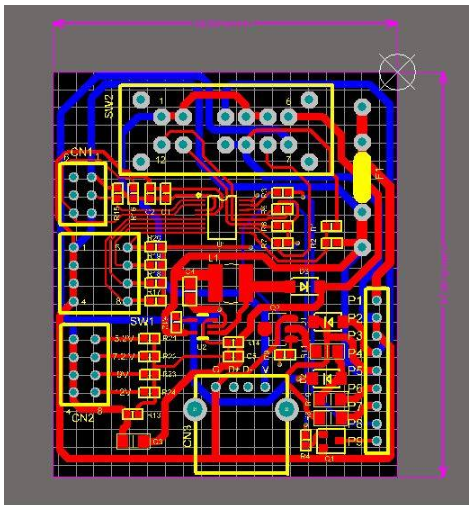
In front of multilayer circuit boards, PCB designers need to determine the adopted circuit board structure according to the circuit scale, size and electromagnetic compatibility (EMC) requirements. After determining the number of layers of the circuit board, they can determine the placement position of the internal electrICal layer and how to distribute different signals on these layers. This is the problem of selecting multilayer PCB stack structures. The stack structure is an important factor affecting the EMC performance of PCB boards, It is also an important means to suppress electromagnetic interference. Now let's understand the key points of the lower stack design.
1. Foil stacking method is recommended for PCB stacking
2. Minimize the use of PP chips and CORE models and types in the same stack (no more than 3 PP stacks per media layer)
3. The thickness of PP medium between two layers should not exceed 21MIL (thick PP medium is difficult to process, and generally an additional core board will lead to an increase in the number of actual PCB layers, thus increasing the production and processing cost of the circuit board)
4. The outer layer (top and bottom layers) of PCB is generally copper foil with thickness of 0.5OZ, and the inner layer is generally copper foil with thickness of 1OZ
Note: Generally, the thickness of copper foil is determined according to the current size and wiring thickness. For example, 2-3OZ copper foil is generally used for power boards, 1OZ copper foil is generally used for ordinary signal boards, and 1/3QZ copper foil may be used for thinner wiring to improve the yield; At the same time, core plates with inconsistent copper foil thickness on both sides shall be avoided in the inner layer.
5. The distribution of PCB wiring layers and plane layers is required to be symmetrical from the centerline to the bottom (including the number of layers, distance from the centerline, copper thickness of wiring layers, etc.)
Note: PCB stacking method shall adopt symmetrical design. Symmetrical design refers to the thickness of insulation layer, type of sEMI solidified sheet, thickness of copper foil, and pattern distribution type (large copper foil layer, circuit layer) as symmetrical as possible relative to the centerline of PCB.
6. The design of line width and dielectric thickness needs to have sufficient margin to avoid SI SIMulation and other design problems caused by insufficient margin
The stack of PCB is composed of power layer, layer and signal layer. The signal layer, as its name implies, is the wiring layer of signal lines. The power layer and stratum are sometiMES collectively referred to as the plane layer.
In a SMAll number of PCB designs, the power and ground plane layer is used for wiring or the power and ground networks are used for wiring. For this mixed type of layer PCB design, it is uniformly calLED the signal layer.
Wave soldering and reflow soldering of pads in pcb design
In PCB design, it is necessary to avoid using a single large bonding pad between two interconnected SMD components, because the solder on the large bonding pad will pull the two PCB components to the middle. The correct approach is to separate the bonding pads of the binary components, and connect the two bonding pads with thinner wires between them. If the wires are required to pass through a larger current, several wires can be connected in parallel;
During t PCB design,here shall be no through-hole on or near the bonding pad of the part, otherwise, in the process, the solder on the PCB bonding pad will flow along the through-hole after melting, resulting in false soldering, less tin, and may flow to the other side of the board to cause short circuit;
PCB design
The types of pin spacing (i.e. pad spacing) between axial devices and jumpers should be reduced as much as possible to reduce the adjustment times of device molding and improve the plug-in efficiency;
resistance soldering paint shall be added between the pads of each pin of the chip IC that needs wave soldering, and solder stealing pads shall be designed at the last pin;
When there are no special requirements for PCB design, the shape of component holes, pads and component pins must match, and the symmetry of pads with respect to the hole center must be ensured (square component pins are equipped with square component holes, square pads; round component pins are equipped with round component holes, round pads), so as to ensure that solder joints are full of tin;
For components that need to be soldered after passing through the tin furnace, the bonding pad should move away from the tin position in the opposite direction to the tin passing direction, and the width of the viewing hole should be 0.5~1.0mm to prevent plugging after passing the wave peak;
Increase the copper sheet, increase the gravitation of the side pin, and facilitate the self centering of reflow soldering.


抖音二維碼

Q Q二維碼

微信二維碼
點擊
然后
聯系
然后
聯系
電話熱線
13410863085Q Q

微信

- 郵箱