鑫景福致力于滿足“快速服務,零缺陷,輔助研發(fā)”PCBA訂購單需求。


PCBA方案設計
The purpose and signifICance of panel design in shenzhen circuit board factory
PCB manufacturers, PCB designers and PCBA manufacturers explain the purpose and significance of panel design
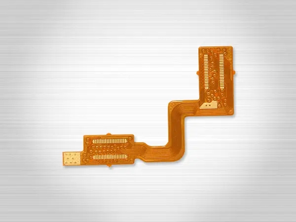
The PCB design is completed because the PCB shape is too SMAll to meet the production process requirements, or a product is composed of several PCBs, so it is necessary to assemble several small boards into a large board with an area meeting the Production requirements, or to assemble multiple PCBs for a product to facilitate the production of electrical equipment. The former is SIMilar to the stamp board. It can not only meet the PCB production process conditions, but also facilitate the electrical installation of components. It is very convenient to separate them when using; The latter is to assemble several sets of PCB boards of a product together, which is convenient for production and is also convenient for a complete set of products.
Shenzhen Circuit board factory assembles several PCB unit boards by various possible connection methods. Usually, when designing a PCB, the hardware designer considers the layout of electrical signals and components on the circuit board, and focuses on the function of the product. The manufacturing and assembly of PCB are considered less. In order to achieve smooth PCB manufacturing, especially in SMT assembly, special attention should be paid to the panel design of PCB Shenzhen Circuit board Factory.
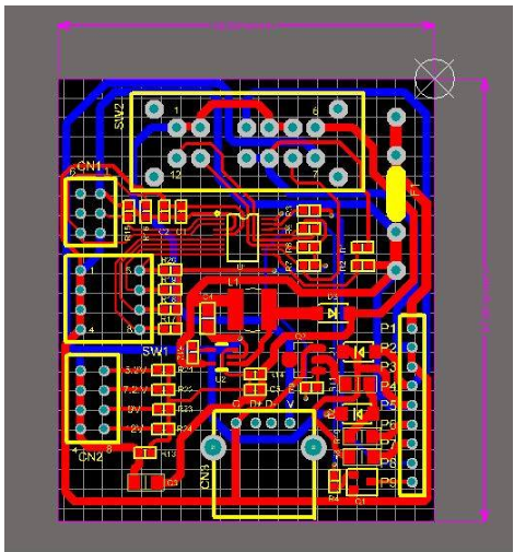
1、 Purpose and significance of Circuit board assembly
To improve the SMT assembly efficiency, the more boards a panel contains, the less the average time for a single PCB to run on the track, and the higher the utilization rate of the mounting equipment, which can greatly improve the SMT production efficiency.
Improve SMT production quality and prevent defective problems in the production process. The distribution density of components on PCB is large. The contour of some components, such as board edge connectors, may exceed the edge of PCB. Before reflow welding or wave soldering is completed, these components are movable. Therefore, additional processes are required to increase the entire PCB panel area to prevent these board edge components from being affected by external factors and reducing the assembly quality.
Easy to operate and prevent damage. The design of panel assembly is also to facilitate the operation of the production line. The assembly of a PCB needs to go through many steps. The finished PCB or sEMI-finished PCB is put into the turnover box, and the turnover rack is used for transfer, storage, storage, transportation, etc. During these operations, specific process edges are required to prevent the components on the PCB from being damaged.
PCB manufacturers, PCB designers and PCBA processors will explain the purpose and significance of panel design.


抖音二維碼

Q Q二維碼

微信二維碼
點擊
然后
聯(lián)系
然后
聯(lián)系
電話熱線
13410863085Q Q

微信

- 郵箱