鑫景福致力于滿足“快速服務,零缺陷,輔助研發”PCBA訂購單需求。


PCBA方案設計
1、 1. PCB schematic element design
If there are required components in the PROTEL catalog, you can directly find them in the schematIC diagram. If there are no required components, you need to
Create a new principle component library (Sch. lib). Process: find the same (or different) number of pins with the required component in the original component library
For a few), PCB components first place component 1 in the schematic editing area (i.e. Schdoc file), click the component, and execute the menu command
Edit | Copy, the cursor becoMES a crosshairs, move the cursor to the component, click the mouse to determine a datum point, and then switch to the
Sch. to be edited Lib file, create a new device (shortcut key create component) in the file and modify the name
Click SCH Lib in the lower right corner of the environment, move the mouse cursor to the empty component name, right-click, and execute in the pop-up shortcut menu
Paste command, paste the component 1 into the new one, and then modify the pin attributes
Then execute the menu command Report | Component Rule Check to perform the gauge check
PCB design
2. PCB schematic design
Create a new schematic file -->load a catalog (including a catalog created by yourself) -->place components -->schematic wiring
Output device report<-- Correct errors -- compile all projects<- Set compile error report options first
(Reports/Bills of Materials)
Output network report (if there is no hierarchical schematic diagram, you can only generate a single document's network report Design/Netlist For Document/Project. If there is a hierarchical module diagram, you need to generate a project's network report Design/Netlist For Project/Project)
In schematIC design, if the circuit diagram is relatively complex, hierarchical schematic design from top to bottom (or from bottom to top) can be adopted
You can use an identical (or SIMilar) encapsulated component to simply modify its attributes to obtain the required component encapsulation. The specific operation process is the process of copying and modifying the component encapsulation from. PCBdoc to. PCBlib. It will not be repeated here No registration required
After component package modification, execute Edit/Set Preference/pin 1 to Set the package reference point at the first pin Then run Report/Component Rule check to set all the rules to be checked, and OK. So far, the encapsulation is complete
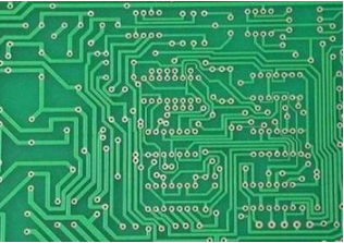
4. PCB design
First, create a new PCB file and import it into the network table when the package lib has been loaded
Automatic component layout Before this step, you need to set the size of the PCB, and you need to plan its size and shape. Click the bottom to select the keep out layer, and then in the place menu, select Draw Line, and then draw a rectangle on the black base plate. You can choose the size yourself.
Note: The drawing line at this time is pink! This indicates that you are planning the board size in the keep out layer.
Then the PCB layout is automatic, and the routing can be carried out smoothly.


抖音二維碼

Q Q二維碼

微信二維碼
點擊
然后
聯系
然后
聯系
電話熱線
13410863085Q Q

微信

- 郵箱