鑫景福致力于滿足“快速服務,零缺陷,輔助研發”PCBA訂購單需求。


PCBA方案設計

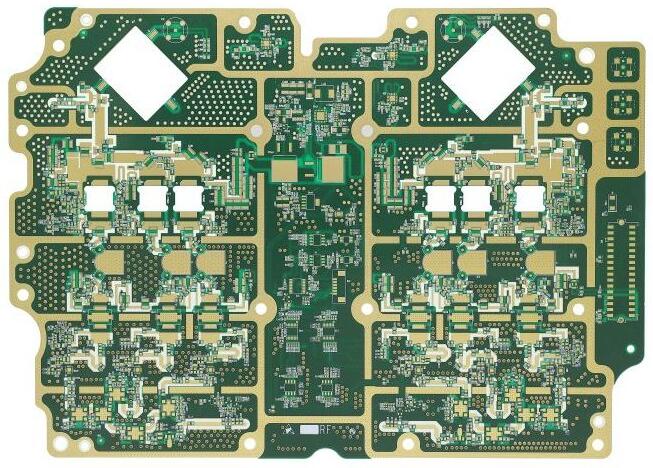
Testing Technology of Multilayer PCB
Packaging density of multilayer PCB increased rapidly Therefore, automatIC detection is necessary and economical even for low density and general number of multilayer PCB boards Two standard methods for detecting multilayer PCB in the complex are needle bed and double probe or flying probe test
1. Needle bed test method
The spring loaded probe connects the method to each detection point on the multilayer PCB board. The spring applies 100-2.00g pressure during each search to ensure good contact at each end. These probes are arranged together, calLED "needle bed". Under the control of the detection software, the detection points and signals can be programmed. Figure 14-3 shows the typical structure of a needle bed tester, which can obtain information about all test points. Only install the probe at the test point to be tested. Although the needle bed test can be used on both sides of the multilayer PCB at the same time, when designing the multilayer PCB, all points should be on the welding side of the multilayer PCB. Needle bed tester is expensive and difficult to maintain. The needle selects different probe arrays according to its specific application.
The main general purpose raster processor consists of a drilled plate spaced 100, 75, or 50 mils on center. This pin is used as a probe and is directly mechanically connected by using the power connector or node on the multilayer pcb board. If the pad on the multilayer PCB matches the test grating, the polyacrylate film perforated according to the specification will be placed between the grating and the multilayer PCB for the design of specific testing. Continuity detection is achieved by accessing the end point of the MESh, which is defined as the X-Y coordinate of the pad. Because each network on the multilayer PCB is detected continuously. This completes the independent test. However, the proximity of the probe limits the effectiveness of the needle bed test.
Flight test

2. Double probe or flight test
The flight pin tester does not depend on the pin pattern mounted on the fixture or bracket. Based on the system, two or more probes are installed on a SMAll free moving magnetic head on the X-Y plane, and the test points are made by CADI
Gerber data is directly controlled. The double probes can move within 4 mils of each other. The probes can move independently without limiting the distance between them. The tester with two movable arms is based on capacitance measurement. Press the multilayer PCB tightly on the insulating layer of the metal plate as another metal plate of the capacitor. If there is a short circuit between lines, the capacitance will be greater than a certain point. If an open circuit occurs, the capacitance will decrease.
Test speed is an important standard for selecting a tester. The needle bed tester can accurately test thousands of test points at a time, while the flying needle tester can only test two or four test points at a time. In addition, the needle bed tester may only need 20-305 for single side testing, depending on the complexity of the circuit board, while the flying needle tester may need Ih or more to complete the same evaluation. Shipley (1991) explained that even though manufacturers of high-yield printed multilayer PCBs think that the mobile flying probe test technology is slow, this method is a good choice for manufacturers of complex multilayer PCBs with low production.
For bare panel testing, there is a special testing instrument (Lea, 1990). A more cost-effective method is to use general instruments, which are more expensive than special instruments at first, but their initial high cost will be offset by the reduction of individual configuration costs. For general purpose gratings, the standard grating for panels with pin assemblies and surface mounted devices is 2.5 mm. At this time, the test pad shall be larger than or equal to 1.3mm. For the Imm grating, the test pad is designed to be greater than 0.7mm. If the grating is very small, the test pin is small, brittle, and easily damaged. In this case, grating larger than 2.5mm is preferred. Crum (1994 b) explained that the combination of the general tester (standard grating tester) and flight tester can make the detection of high-density multilayer PCB accurate and economical. Another method he suggests is to use a conductive rubber tester, which can be used to detect points that deviate from the grating. However, different pad heights and hot air leveling will hinder the connection of test points.
There are generally 3 detection levels:
1) Bare panel detection;
2) Online detection;
3) Function test.
The universal tester can be used to test a class of styles and types of multilayer PCB boards, as well as to test special applications.
The above is the explanation given by the editor of pcb circuit board company.
If you want to know more about PCBA, you can go to our company's home page to learn about it.
In addition, our company also sells various circuit boards,
High Frequency Circuit Board and SMT chip are waiting for your presence again.


抖音二維碼

Q Q二維碼

微信二維碼
點擊
然后
聯系
然后
聯系
電話熱線
13410863085Q Q

微信

- 郵箱