鑫景福致力于滿足“快速服務,零缺陷,輔助研發”PCBA訂購單需求。


PCBA方案設計

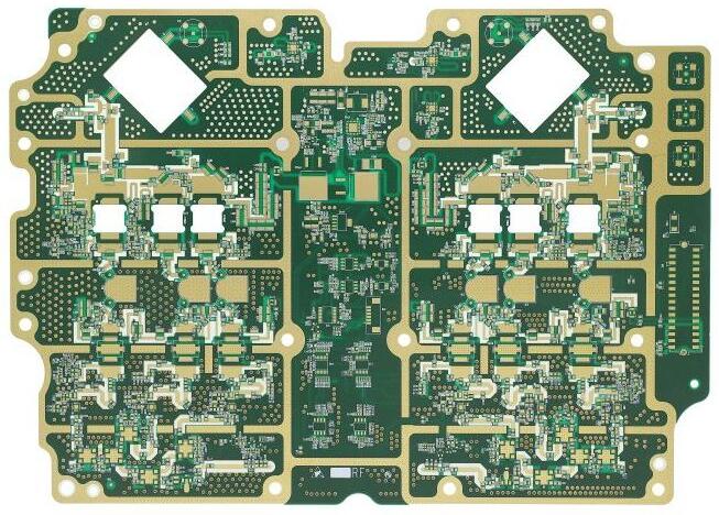
Why use gold impregnated PCB?
Surface treatment of printed circuit board
Anti oxidation OSP, tin spraying, lead-free tin spraying, immersion gold, tin DIPping, silver sinking, hard gold plating, full plate gold plating, gold finger, nICkel palladium outsourcing service provider: lower cost, good solderability, poor storage conditions, short time, environmental protection technology, good welding, smooth Tin spraying: tin spraying boards are generally multi-layer (4-46 layers) high-precision PCB models, which have been used by many large doMEStic communication companies, computers, Medical Equipment, aerospace companies and research organizations The golden finger is a memory stick It is used as the connecting part between the upper part and the memory slot. All signals are transmitted through the golden finger The golden finger is composed of many golden conductive contacts. Because its surface is gold-plated and its conductive contacts are arranged like fingers, it is calLED the "golden finger" The gold finger is actually coated with a layer of gold on the CCL through a special process, because the gold has strong oxidation resistance and strong conductivity However, due to the high price of gold, most memories are replaced by tin plating Tin materials have been very popular since the 1990s Moreover, at present, the "golden finger" of the motherboard, memory and graphics card are almost all tin data Only some high-performance server/workstation accessory contacts will continue to be gilded, which is naturally expensive
PCB board

Why should I use a gold plate
Like this integrated circuit, the integration is getting higher and higher, and IC pins become more dense The vertical tin spraying process is difficult to flatten the thin pads, which makes it difficult to place SMT; In addition, the standby life of tin stencil is very short The gold-plated plate just solves these problems:
For surface mount process, it is especially suitable for 0603 and 0402 ultra SMAll surface mount, because the flatness of the pad is directly related to the quality of solder paste printing process, which has a decisive impact on the quality of subsequent reflow soldering Therefore, the whole circuit board is gold plated It is common in high-density and subminiature Surface Mount Technology In the trial production stage, due to factors such as component procurement, the board of directors is usually not held as soon as possible Welding, but it usually requires several weeks or even months before use. The standby life of gold plate is several times that of lead tin alloy, so everyone is willing to use it In addition, the cost of gold plated PCB in the sample stage is almost the same as that of lead tin alloy plate However, as the lines become more dense, the line width and spacing have reached 3-4 MIL Therefore, with the increase of signal frequency, the problem of gold wire short circuit appears The interest rate is getting higher and higher. Due to the skin effect, the signal transmission in multi-layer electroplating has more obvious influence on the signal quality Skin effect refers to: high-frequency alternating current, the current will tend to concentrate on the surface of the wire to flow According to the calculation, the skin depth is related to the frequency
Why to use immersion gold plate
In order to solve the above problems of gold plated boards, PCB circuit boards using gold impregnated boards mainly have the following characteristics:
Because the crystal structure formed by gold immersion and gold plating is different, gold immersion is yellower than gold plating, and customers will be more satisfied Because the crystal structures formed by gold dipping and gold plating are different, gold dipping is easier to weld than gold plating and will not lead to poor welding and customer complaints Because there is only nickel and gold on the gold dipping plate, the signal transmission in the skin effect will not affect the signal on the copper layer Because there is only nickel and gold on the pad of the gold impregnated plate, it will not produce gold wire and cause slight short circuit Because there is only nickel and gold on the bonding pad of the gold impregnated plate, the bonding between the solder mask and the copper layer on the circuit is stronger During compensation, the project will not affect the spacing Because the crystal structures formed by immersion and gold plating are different, the stress of immersion gold plating plate is easier to control, and it is more conducive to bonding processing for bonded products At the same time, this is precisely because immersion gilding is softer than gold plating. In retrospect, immersion gilding plates are not as wear-resistant as gold fingers The flatness and standby life of the gilded plate are as good as those of the gilded plate
PCB board
Gilded plate and gilded plate
In fact, there are two kinds of gold plating processes: one is electrogilding, the other is immersion gold Used in the gold plating process, the effect of tin plating is greatly reduced, and the effect of gold immersion tin plating is better; Unless the manufacturer requires binding, most manufacturers will now choose the gold leaching process Generally, the surface treatment of pcb circuit board is as follows: gold plating (electrogilding, gold deposition), silver plating, OSP, tin spraying (lead and lead-free), which are mainly used for FR-4 or CEM-3 boards, paper based materials and rosin coating surface treatment methods; Poor tin (poor tin), if the production and information technology reasons of solder paste and other chip manufacturers are excluded
This is only for PCB problems. The reasons are as follows:
When printing PCB, whether there is oil permeable film surface at the pot position, which can block the effect of tin plating; This can be verified by tin bleaching test Whether the lubrication position of the disc bit meets the design requirements, that is, whether the gasket design can fully ensure the supporting effect of the parts Whether the liner is polluted can be obtained through ion pollution test; The above three points are basically the key aspects considered by PCB manufacturers As for the advantages and disadvantages of several surface treatment methods, everyone has his own advantages and disadvantages In terms of gold plating, it can keep the PCB for a longer time, the temperature and humidity of the external environment change less (compared with other surface treatments), and it can generally be stored for about a year; Secondly, the surface treatment of tin spraying and OSP are stored in the environment
Temperature and humidity
Pay attention to time. Under normal circumstances, the surface treatment of PCB immersed in silver is slightly different, the price is also high, the storage conditions are higher, and sulfur free paper is required for packaging


抖音二維碼

Q Q二維碼

微信二維碼
點擊
然后
聯系
然后
聯系
電話熱線
13410863085Q Q

微信

- 郵箱