鑫景福致力于滿(mǎn)足“快速服務(wù),零缺陷,輔助研發(fā)”P(pán)CBA訂購(gòu)單需求。


PCBA方案設(shè)計(jì)
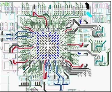
Layout is the first problem for pcb design engineers. This problem depends on some contents in the drawing, and some devICes need to be set together based on logical considerations. However, it should be noted that temperature sensitive elements, such as sensors, should be set separately from heat generating elements, including power converters. For designs with multiple power settings, 12V and 15V power converters can be set at different positions of the circuit board, because the heat and electronic noise generated by them will affect the reliability and performance of other components and circuit boards.
The above PCB components will also affect the electromagnetic performance of, which is not only important for the performance and energy consumption of the circuit board, but also has a great impact on the economy of the circuit board. Therefore, all circuit board equipment sold in Europe must obtain the CE MARK to prove that it will not interfere with other systems. However, this is usually only from the perspective of power supply. There are also many devices that EMIt noise, such as DC-DC converters and high-speed data converters. Due to the defects in the design of the circuit board, these noises can be captured by the channel and radiated as a SMAll antenna, thus generating noise and abnormal frequency areas.
The problem of far field electromagnetic interference (EMI) can be solved by installing filters at noise points or using metal enclosures to shield signals. However, due attention should be paid to the equipment that can release electromagnetic interference (EMI) on the circuit board, which allows the circuit board to choose a cheaper shell, thus effectively reducing the cost of the entire system.
In the process of circuit board design, electromagnetic interference (EMI) is indeed a factor that must be paid attention to. Electromagnetic crosstalk can couple with the channel, which disrupts the signal into noise and affects the overall performance of the circuit board. If the coupling noise is too high, the signal may be completely covered. Therefore, more expensive signal amplifiers must be instalLED to restore normal. However, if the signal circuit layout can be fully considered at the beginning of the circuit Board Design, the above problems can be avoided. Because the design of the circuit board will be different according to different devices, different places of use, different heat dissipation requirements, and different electromagnetic interference (EMI) conditions, the design template will come into use.
Capacitance is also an important issue in circuit board design that cannot be ignored, because capacitance will affect the propagation speed of signals and increase the consumption of electricity. The channel will couple with the adjacent line or cross two circuit layers vertically, thus forming a capacitor unintentionally. The above problems can be solved relatively easily by reducing the length of parallel lines and installing kinks on one of the lines to cut off the coupling. However, this also requires PCB engineering designers to fully consider the production design principles to ensure that the PCB design scheme is easy to manufacture and avoid any noise radiation caused by excessive bending angle of the circuit. The distance between lines may also be too close, which will create a short circuit between lines, especially at line bends. As time goes on, metal "whiskers" will appear. Design rule detection can usually identify areas where the loop risk is higher than normal.
This problem is particularly prominent in the design of the ground plane. A metal circuit layer may form coupling with all lines above and below it. Although the metal layer can effectively block noise, it will also generate associated capacitance, affect the running speed of the line, and increase power consumption.
As far as the design of multilayer circuit boards is concerned, the design of through-hole between different layers of circuit boards is probably the most controversial issue, because through-hole design will bring many problems to the production and manufacturing of circuit boards. The through-hole between the circuit board layers will affect the performance of the signal and reduce the reliability of the circuit board design, so it should be given full attention.
Solution
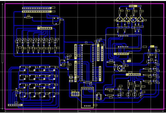
In the design process of Printed Circuit Board (PCB), many different methods can be adopted to solve various problems. The adjustment of the existing design scheme itself, such as adjusting the line layout to reduce noise; There are also methods for PCB layout. The design components can be automatically installed through the layout tool, but if the automatic layout can be manually adjusted, it will help to improve the quality of the circuit board design. Through this measure, design rule detection will rely on technical documents to ensure that the design of the circuit board can meet the requirements of the circuit board manufacturer.
Separating different circuit board layers can reduce the associated capacitance. However, this will increase the number of layers of the circuit board, thus increasing the PCB proofing cost and bringing more problems in through-hole. Although the use of orthogonal grid power supply system and grounding circuit design may increase the physical size of the circuit board, it can effectively play the role of the grounding layer in the double-layer circuit board and reduce the capacitance and the complexity of circuit board production.
Design tools, including DesignSpark PCB, can help engineering designers solve many problems at the beginning of design, but engineering designers still need to have a full understanding of the design requirements of printed circuit boards (PCBs). For example, if the editor of a printed circuit board (PCB) needs to know the number of layers of the PCB at the beginning of the design, for example, a double-layer circuit board needs to have a ground plane and a power supply plane, and two mutually independent board layers. Automatic component layout technology is very useful. It can help designers spend more time to design the layout area of equipment. For example, if the power supply equipment is too close to sensitive signal lines or areas with high temperature, many problems will arise. SIMilarly, signal lines can also be automatically routed to avoid most problems. However, analysis and manual operation of high-risk areas will help greatly improve the quality of PCB design, increase revenue and reduce overall cost.


抖音二維碼

Q Q二維碼

微信二維碼
點(diǎn)擊
然后
聯(lián)系
然后
聯(lián)系
電話(huà)熱線(xiàn)
13410863085Q Q

微信

- 郵箱