鑫景福致力于滿足“快速服務(wù),零缺陷,輔助研發(fā)”PCBA訂購單需求。


PCBA方案設(shè)計

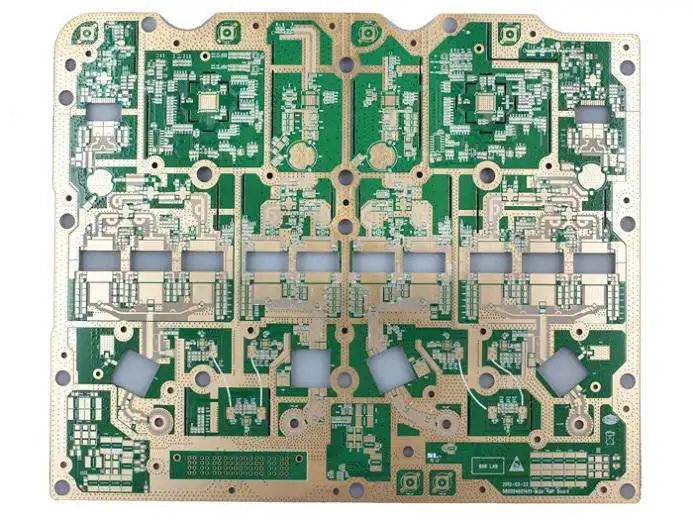
How to maintain high effICiency in SMT chip processing
1. The MARK point is round or square, with a diameter of 1.0mm, which can be determined according to the SMT equipment. The copper area from the mark point to the surrounding area must be greater than 2.0mm. The mark point is not allowed to be creased, dirty, exposed copper, etc;
2. Each large board must have Mark points at four corners or two Mark points at opposite corners, and the distance from the Mark point to the edge must be greater than 5mm;
3. Each SMAll board must have two Mark points; 4. According to the specific equipment and efficiency evaluation, "X" plate is not allowed in FPC panel;
5. When mending the board, use wide adhesive tape to firmly stick the board and the board, and then check the film. If the mended board is not flat, it must be pressurized again, and then check the film again;
6. The bonding pad spacing of 0402 component is 0.4mm; The bonding pad spacing of 0603 and 0805 components is 0.6 mm; The bonding pad should preferably be square;
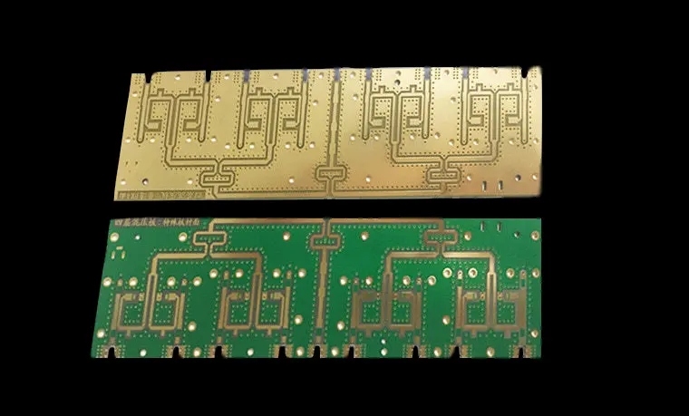
7. In order to avoid sinking of small area of FPC board due to punching, punching from the bottom direction; 8. After FPC board is made, it must be vacuum packed after baking; Before SMT goes online, it is better to pre bake;
9. The optimal panel size is within 200mm × 150mm; 10. Four SMT fixture positioning holes shall be reserved at the edge of the panel, with the hole diameter of 2.0mm;
11. The minimum distance between the edge elements of the panel and the panel edge is 10mm; 12. Distribution of panels: Each small panel shall be distributed in the same direction as far as possible;
13. The gold finger area (i.e. hot pressing end and solderable end) of each small plate shall be assembLED into one piece to prevent the gold finger from eating tin in SMT production;
14. The minimum distance between pads of chip components is 0.5mm.

Engineering designers and technologists are expected to have such experience: after FPC production is completed, SMT welding is required for upper components; The problem is that as an excellent designer, he can maintain high quality and efficiency in the smt production process because he knows some special requirements about the SMT process in advance. Because FPC has a high requirement on the flatness of the board itself in the SMT process; In addition, the spacing, MARK point setting, panel size, etc. will affect the quality and efficiency of SMT. Therefore, as a design engineer of FPC manufacturer, he should know more about some special requirements of SMT and consider the design comprehensively before manufacturing in combination with FPC's manufacturing process capability. He should not be afraid of one thing and lose another, otherwise the future will be endless.


抖音二維碼

Q Q二維碼

微信二維碼
點擊
然后
聯(lián)系
然后
聯(lián)系
電話熱線
13410863085Q Q

微信

- 郵箱