鑫景福致力于滿足“快速服務(wù),零缺陷,輔助研發(fā)”PCBA訂購(gòu)單需求。


PCBA方案設(shè)計(jì)
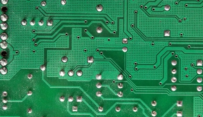
Discussion on the Wiring Problem of High Speed PCB from the Angle of PractICe
PCB (printed circuit board) wiring plays a key role in high-speed circuits. This paper mainly discusses the wiring problem of high-speed circuit from the perspective of practice. The main purpose is to help new users pay attention to a variety of different issues that need to be considered when designing high-speed circuit PCB routing. Another purpose is to provide a review material for customers who have not touched PCB wiring for some time. Due to the limited layout, it is impossible to discuss all the problems in detail in this paper, but we will discuss the key parts that have the greatest effect on improving circuit performance, shortening design time and saving modification time.
Although this paper mainly focuses on the circuits related to high-speed operational amplifiers, the problems and methods discussed here are generally applicable to the wiring of most other high-speed analog circuits. When the operational amplifier works in a very high RF band, the performance of the circuit largely depends on PCB wiring. High performance circuit design that looks good on the "drawing" can only achieve ordinary performance if it is affected by careless wiring. Anticipating and paying attention to important details throughout the wiring process will help ensure the expected circuit performance.
schematic diagram
Although good schematics cannot guarantee good wiring, good wiring starts with good schematics. When drawing the schematic diagram, you must think carefully and consider the signal flow direction of the whole circuit. If there is a normal and stable signal flow from left to right in the schematic diagram, then there should be the same good signal flow on the PCB. Give as much useful information as possible on the schematic diagram. Because sometiMES the circuit design engineer is absent, customers will ask us to help solve the circuit problems. Designers, technicians and engineers engaged in this work will be very grateful, including us.
In addition to the common reference identifier, power consumption and error tolerance, what information should be given in the schematic diagram? Here are some suggestions to turn a common schematic into a first-class schematic. Add waveform, mechanical information about housing, length of printed wire and blank area; Indicate which components need to be placed on the PCB; Give adjustment information, component value range, heat dissipation information, control impedance printed wire, notes, brief circuit action description... (and others).
Don't believe anyone
If you do not design the wiring yourself, be sure to leave plenty of time to carefully check the design of the wiring designer. At this point, a SMAll precaution is worth a hundred times the remedy. Don't expect the cabling person to understand your idea. Your advice and guidance is most important at the beginning of the cabling design process. The more information you can provide and the more you intervene in the whole wiring process, the better the PCB will be. Set a tentative completion point for the cabling design engineer - quickly check according to the cabling progress report you want. This "closed loop" method can prevent wiring from going astray, thus minimizing the possibility of rework.
The instructions to the wiring engineer include: a brief description of the circuit function, a PCB sketch indicating the input and output positions, PCB stack information (for example, how thick the board is, how many layers are there, and the details of each signal layer and grounding plane - power consumption, ground wire, analog signal, digital signal and RF signal); What signals are required for each layer; The placement position of important components is required; The exact location of the bypass element; Which printed lines are important; Which lines need to control impedance printed lines; Which lines need matching length; Dimensions of elements; Which printed wires need to be away from (or close to) each other; Which lines need to be away from (or close to) each other; Which components need to be away from (or close to) each other; Which components should be placed on the top and which on the bottom of the PCB. Never complain that you need to give too much information to others - too little? Yes; Too much? no
One learning experience: About 10 years ago, I designed a multilayer surface mount circuit board - there are components on both sides of the board. Many screws are used to fix the board in a gold-plated aluminum housing (because there is a very strict shockproof index). The pins that provide offset feedthrough pass through the board. The pin is connected to the PCB through a solder wire. This is a very complicated device. Some components on the board are used for test setup (SAT). But I have specified the location of these elements. Can you guess where these components are instalLED? By the way, it's under the board. When product engineers and technicians had to disassemble the whole device and reassemble it after setting, they were very unhappy. I have never made such mistakes since then.
position
Just as in a PCB, position determines everything. It is very important to place a circuit on a PCB, to install its specific circuit components, and to identify other adjacent circuits.
Usually, the positions of input, output and power supply are predetermined, but the circuits between them need to "give play to their creativity". This is why paying attention to the details of cabling can pay off handsomely. Start from the position of key components, and consider according to the specific circuit and the entire PCB. Specifying the location of key components and the path of signals from the beginning helps to ensure that the design achieves the desired work objectives. Getting the right design once can reduce cost and pressure - and shorten the development cycle.
bypass source
It is a very important aspect in PCB design to bypass the power supply of the amplifier in order to reduce noise, including high-speed operational amplifiers or other high-speed circuits. There are two common configuration methods for bypass high-speed operational amplifiers.
Power supply terminal grounding: This method is the most effective in most cases. Multiple parallel capacitors are used to directly ground the power supply pin of the operational amplifier. In general, two shunt capacitors are sufficient - but adding shunt capacitors may benefit some circuits.
Shunting capacitors with different capacitance values helps ensure that the power supply pin can only see very low AC impedance in a very wide frequency band. This is especially important at the attenuation frequency of the power supply rejection ratio (PSR) of the operational amplifier. This capacitor helps compensate for the reduced PSR of the amplifier. Maintaining a low impedance ground path over many octave ranges will help ensure that harmful noise does not enter the op amp.
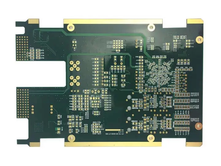
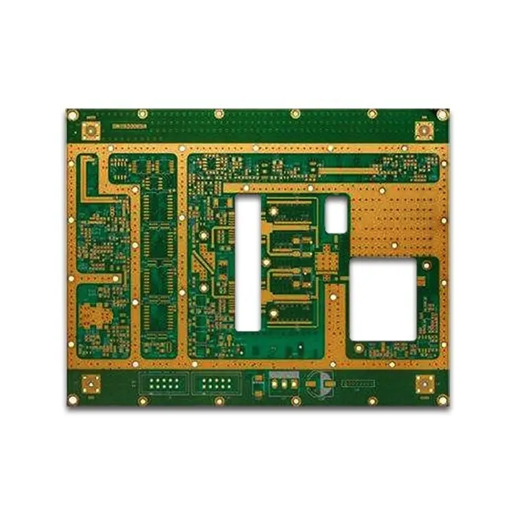
PCB manufacturers, PCB designers and PCBA manufacturers will explain how to discuss high-Speed PCB wiring from a practical perspective.


抖音二維碼

Q Q二維碼

微信二維碼
點(diǎn)擊
然后
聯(lián)系
然后
聯(lián)系
電話熱線
13410863085Q Q

微信

- 郵箱