鑫景福致力于滿足“快速服務,零缺陷,輔助研發”PCBA訂購單需求。


PCBA方案設計
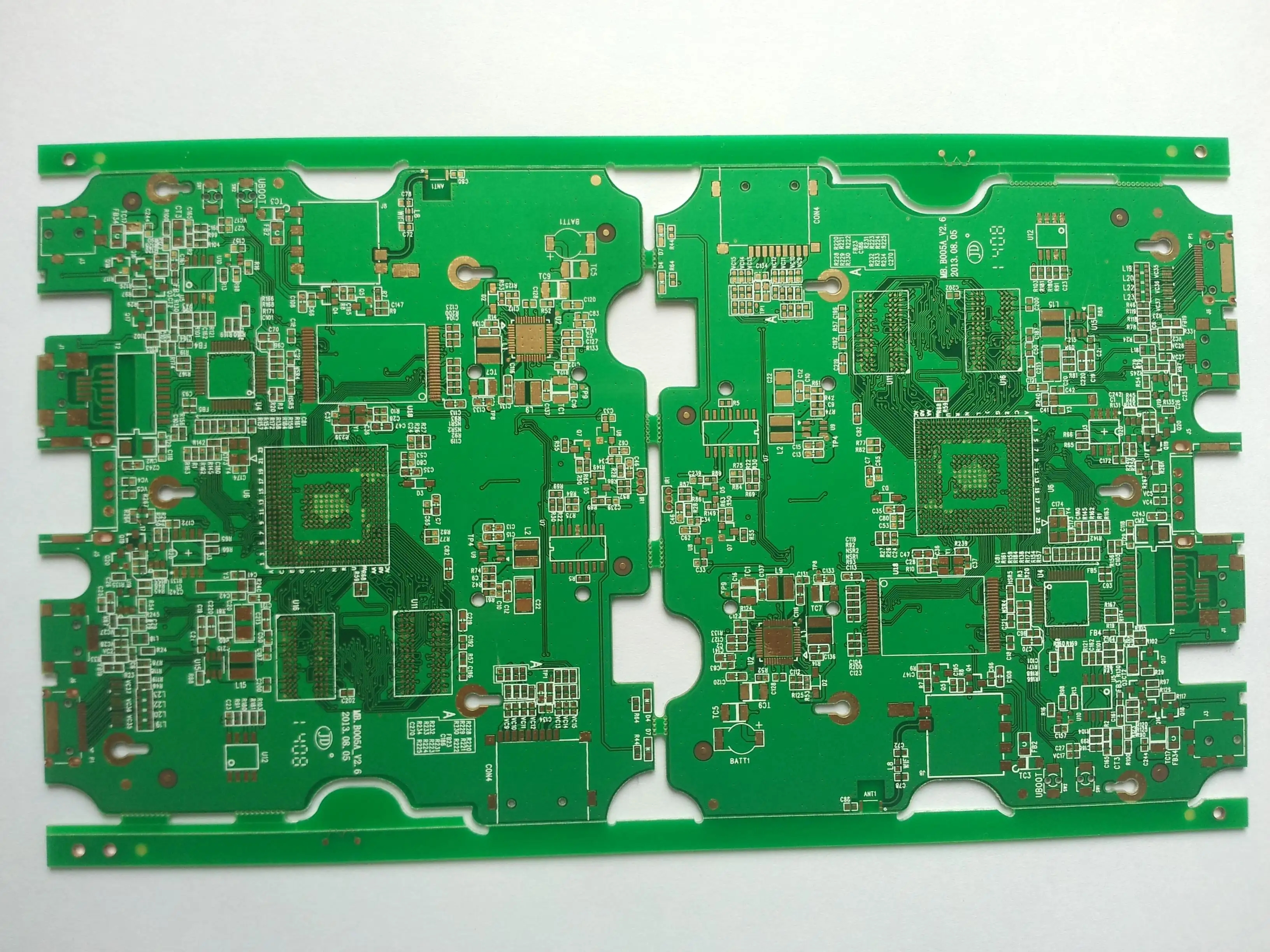
The Delay Problem of High Speed Circuit Board Design and EMC
PCB manufacturers, PCB designers and PCBA manufacturers explain the delay problem of high-speed PCB design and EMC
delay
During SIMulation, the capacitance of components and packages (and sometiMES inductance) should be considered. Two problems should be noted. First, the simulator may not be able to correctly simulate distributed capacitors; Secondly, we should also pay attention to the impact of different production conditions on the incomplete level and non parallel routing. Many field solution tools cannot analyze the stack distribution without full power or ground layers. However, if the signal layer is adjacent to a ground wire layer, the calculated delay will be very bad. For example, the capacitance will have the maximum delay; If both layers of a double-sided board are covered with many ground wires and VCC copper foils, this situation is more serious. If the process is not automated, it will be very messy to set these things in a CAD system.
EMC
EMC has many influencing factors, many of whICh are usually not analyzed. Even if they are analyzed, it is often too late after the design is completed. Here are some factors that affect EMC:
1. The slot of the power layer will form a quarter wavelength antenna. Drilling method shall be used to replace the occasion where the installation slot is required on the metal container.
2. Inductive element. I once met a designer who followed all the design rules and made simulations, but his circuit board still had a lot of radiation signals. The reason is that two inductors on the top layer are placed in parallel with each other, forming a transformer.
3. Due to the influence of incomplete grounding layer, the low impedance of the inner layer causes large transient current of the outer layer.
Using defensive design can avoid most of these problems. First of all, we should make the correct stack structure and routing strategy, so that we have a good start.
Some basic problems are not involved here, such as network topology, causes of signal distortion and crosstalk calculation methods; It only analyzes some sensitive issues to help readers apply the results obtained from the EDA system. Any analysis depends on the model used, and factors that cannot be analyzed will also affect the results. Too complex is just like too imprecise, avoiding too many parameter changes (such as printed line width), which is conducive to neat and consistent design.
PCB manufacturers, PCB designers and PCBA manufacturers explain the delay problem of high-Speed PCB design and EMC


抖音二維碼

Q Q二維碼

微信二維碼
點擊
然后
聯系
然后
聯系
電話熱線
13410863085Q Q

微信

- 郵箱