鑫景福致力于滿足“快速服務,零缺陷,輔助研發”PCBA訂購單需求。


PCBA方案設計

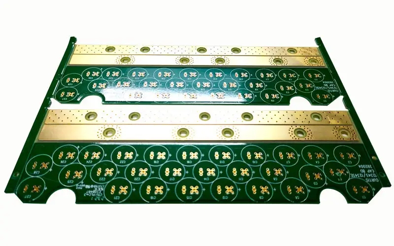
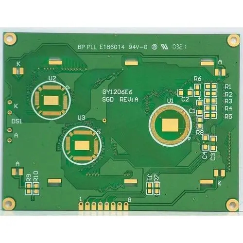
PCB wiring Rules and Grounding Methods in PCB Design
The rules of PCB wiring are as follows:
1) Thread length
The copper film wire should be as short as possible, especially in high-frequency circuits. The corner of the copper film wire shall be rounded or beveLED, while the right angle or sharp corner will affect the electrICal performance in the case of high frequency circuit and high wiring density. When wiring the double-sided boards, the wires on both sides should be perpendicular, oblique or bent to avoid parallel to each other to reduce parasitic capacitance.
2) Lineweight
The width of copper film wire shall meet the requirements of electrical characteristics and be convenient for production. Its minimum value depends on the current flowing through it, but generally should not be less than 0.2mm. As long as the plate area is large enough, the width and spacing of copper film wire should preferably be 0.3mm. Generally, the line width of 1~1.5mm allows the current to flow through 2A. For example, the wire width greater than 1mm should be selected for ground wire and power wire. When two lines are laid between the pads of the integrated circuit base, the pad diameter is 50 mil, and the line width and line spacing are 10 mil. When one line is laid between pads, the pad diameter is 64 mil, and the line width and line spacing are 12 mil. Note the conversion between metric system and imperial system, 100mil=2.54mm.
3) Line spacing
The spacing between adjacent copper film wires shall meet the electrical safety requirements, and in order to facilitate production, the wider the spacing, the better. The minimum spacing shall at least be able to withstand the peak value of the applied voltage. In the case of low wiring density, the spacing should be as large as possible.
4) Shielding and grounding
The common ground wire of the copper film wire should be placed at the edge of the circuit board as much as possible. Copper foil should be reserved as much as possible on the PCB as a ground wire to enhance the shielding ability. In addition, the shape of the ground wire should be made into a loop or grid. Multilayer PCB board uses the inner layer as the special layer for power supply and ground wire, so it can play a better shielding effect.
PCB board grounding
1. Common impedance interference of ground wire
The ground wire on the circuit diagram represents the zero potential in the circuit and serves as the common reference point for other points in the circuit. In the actual circuit, the existence of the ground wire (copper film wire) impedance will inevitably lead to common impedance interference. Therefore, when wiring, the points with the ground wire symbol cannot be connected together, which may cause harmful coupling and affect the normal operation of the circuit.
2. How to connect the ground wire
Generally, in an electronic system, ground wires are divided into system ground, enclosure ground (shield ground), digital ground (logic ground) and analog ground. The following points should be noted when connecting ground wires:
1) Correct selection of single point grounding and multi-point grounding
In low-frequency circuits, the signal frequency is less than 1MHz, the inductance between wiring and components can be ignored, and the voltage drop generated on the resistance of the ground circuit has a great impact on the circuit, so the single point grounding method should be adopted. When the signal frequency is greater than 10MHz, the influence of the ground wire inductance is large, so the multi-point grounding method of nearby grounding should be adopted. When the signal frequency is between 1~10MHz, if the single point grounding method is adopted, the length of the ground wire should not exceed 1/20 of the wavelength, otherwise the multi-point grounding should be adopted.
2) Digital and analog separation
There are both digital circuits and analog circuits on the PCB board. They should be separated as far as possible, and the ground wires should not be mixed. They should be connected to the ground wire end of the power supply separately (preferably the power supply end is also connected separately). Try to increase the area of linear circuit. Generally, digital circuits have strong anti-interference capability. The noise tolerance of TTL circuits is 0.4~0.6V. The noise tolerance of CMOS digital circuits is 0.3~0.45 tiMES of the power supply voltage. However, the analog circuits can work abnormally as long as there is a microvolt level noise. Therefore, the two types of circuits should be laid and wired separately.
3) Try to thicken the ground wire
If the ground wire is very thin, the ground potential will change with the change of current, causing interference to the signal of the electronic system, especially the analog circuit. Therefore, the ground wire should be as wide as possible, generally more than 3mm.
4) Make the grounding wire into a closed loop
When there are only digital circuits on the PCB board, the ground wire should form a loop, which can significantly improve the anti-interference capability. This is because when there are many integrated circuits on the PCB board, if the ground wire is very thin, it will cause a large ground potential difference, and the ring ground wire can reduce the ground resistance, thereby reducing the ground potential difference.
5) Grounding of the same level circuit
The grounding point of the circuit at the same level should be as close as possible, and the power filter capacitor of the circuit at this level should also be connected to the grounding point at this level.
6) Grounding method of general ground wire
The general ground wire must be connected from weak current to strong current level by level in strict accordance with the sequence of high frequency, medium frequency and low frequency. The high-frequency part should preferably adopt a large area of enclosed ground wire to ensure a good shielding effect.
PCB manufacturers, PCB designers and PCBA manufacturers explain PCB wiring rules and grounding methods in PCB design.


抖音二維碼

Q Q二維碼

微信二維碼
點擊
然后
聯系
然后
聯系
電話熱線
13410863085Q Q

微信

- 郵箱