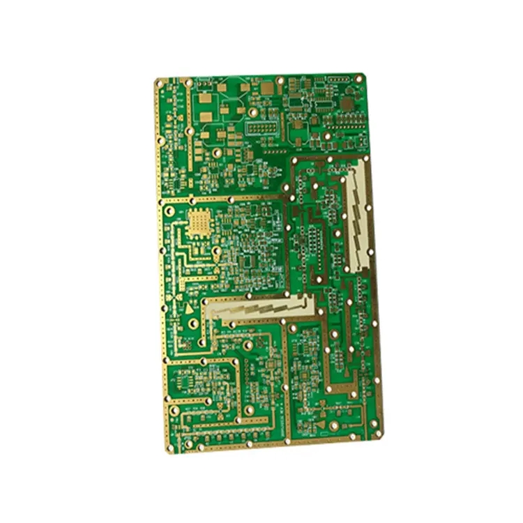
鑫景福致力于滿足“快速服務,零缺陷,輔助研發”PCBA訂購單需求。


PCBA方案設計
How to Draw Differential Pairs with Excellent Performance in High Quality PCB Manufacturing
PCB manufacturers, PCB designers and PCBA manufacturers explain how to draw differential pairs with excellent performance in high-quality PCB manufacturing
Before explaining the importance of difference to wiring, first understand the factors affecting transmission line impedance: line width, line length, line thICkness, side wall shape, solder mask coverage and transmission line medium are obvious factors. The dielectric constant and dielectric thickness will also affect the accuracy of transmission line impedance. Please refer to the relevant books on signal integrity analysis for the specific calculation formula. Knowing these influencing factors can help us design a good routing, especially when it is necessary to define the routing impedance, and adjust the routing width and thickness through relevant software to complete the routing of fixed impedance.
The differential pair is calLED differential pair because the signal transmitted on it is equal to the difference between two complementary and mutually referenced signals, which can greatly reduce external interference. The wiring of differential pairs should be properly close and parallel. The so-called appropriate approach is because this distance will affect the value of differential impedance, which is an important parameter for designing differential pairs. Parallel routing is required. In the circuit design, if all the signal lines are single ended and the impedance design is done well, the system can normally work. Once the ground potentials at both ends of the signal line are different, or even the gap is large, the system will not work properly. However, differential pair wiring or routing is an effective solution. Because the difference line has equal length, equal impedance, and passes through approximately the same environment, it has an inherent advantage in stabilizing signals.
In the schematIC design, the differential signal is usually MARKed with "_N" and "_P" as the dropout. The differential line can effectively solve the problem that there is no good reference ground connection between the signal source and the load, suppress the interference of electronic products and reduce the electromagnetic interference (EMI) generated by the signal line.
So, why can the difference line effectively eliminate noise? First of all, let's take a look at the general requirements when distributing the difference line: the difference line should be designed to ensure that the length of the two lines is equal, usually within 5%. It is a good design experience to have a distance of 3w between the two difference lines and to wrap the ground around the difference line. In this way, on the one hand, the magnetic fields generated by the two signal lines of the difference line cancel each other to reduce EMI; On the other hand, if external noise interference signal is introduced into the differential pair signal line at the same time, because its differential result is taken, the noise can be eliminated very well, which is SIMilar to the classical three op amp amplifier.
For the common differential mode terminal matching resistance, we usually choose 50 ohm or 100 ohm, and further matching is required in practice. Since the signals transmitted in differential mode are mutual references and independent of the ground, there is no common mode RF energy. It can also be determined as common mode differential mode at the beginning of the design and compared with different modes in the later debugging process, which is also a good method.
When plotting the routing of differential pairs of PCBs, try to route on the same layer. The layer change of differential pair routing will introduce impedance discontinuity due to the increase of vias. Secondly, if the layer change also makes the loop current without a good low impedance loop, there will be an RF loop. If the differential pair is long, the common mode RF energy will be affected. Another reason is that the differential pair has different signal transmission speeds between different layers. In the data related to signal integrity analysis, it can be seen that the signal transmission on the microstrip line is faster than that on the stripline, which will also cause a certain time delay. In connection, pay attention to the connection of differential pairs. If the load is not a direct load but a capacitive load, EMI may be introduced. In circuit design, we also need to pay attention to the impedance matching of the terminal to prevent EMI problems caused by transmission reflection.
PCB manufacturers, PCB designers and PCBA processors will explain how to draw differential pairs with excellent performance in high-quality PCB manufacturing.


抖音二維碼

Q Q二維碼

微信二維碼
點擊
然后
聯系
然后
聯系
電話熱線
13410863085Q Q

微信

- 郵箱