鑫景福致力于滿足“快速服務(wù),零缺陷,輔助研發(fā)”PCBA訂購單需求。


PCBA方案設(shè)計
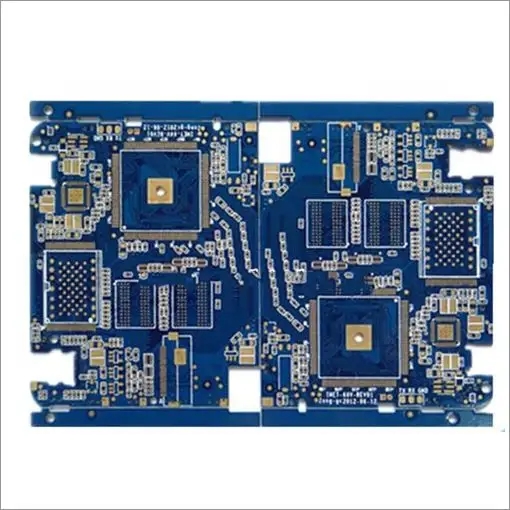
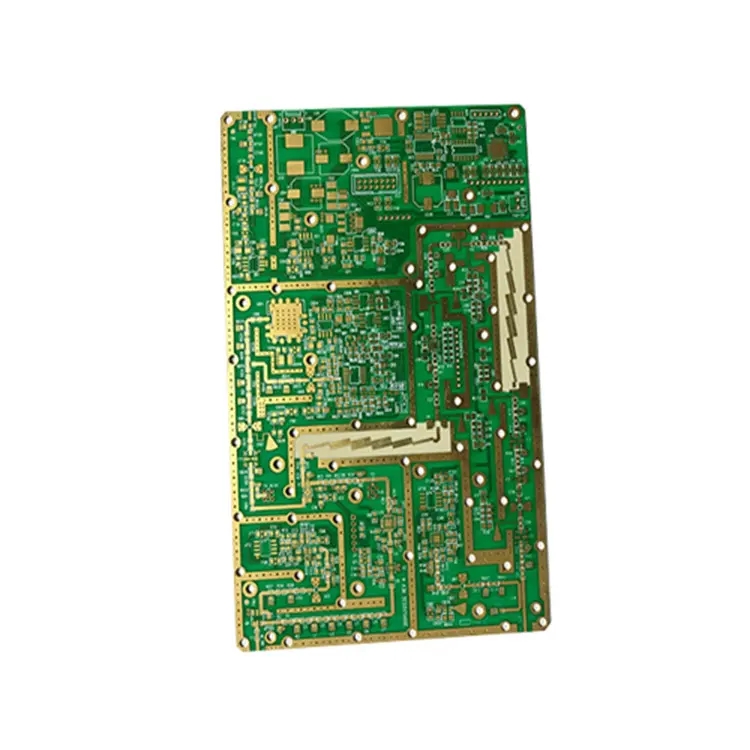
The circuit board manufacturer tells you how to reverse the schematIC diagram
In the research of PCB reverse technology, the reverse schematic refers to the reverse deduction of PCB circuit diagram based on the PCB file diagram or the direct drawing of PCB circuit diagram based on the actual product, which is intended to explain the principle and working condition of PCB. Moreover, this circuit diagram is also used to analyze the functional characteristics of the product itself. In the forward design, general product R&D should first carry out schematIC design, and then carry out PCB design according to the schematic.
PCB schematics play a special role whether they are used to analyze PCB principles and product working characteristics in reverse research or as the basis and basis of PCB design in forward design. Then, how to reverse the PCB schematic diagram according to the document diagram or real object, and what details should be paid attention to in the reverse process?
1、 Reasonably divide functional areas
When reverse designing the schematic diagram of a good PCB, reasonable division of functional areas can help engineers reduce some unnecessary trouble and improve the efficiency of drawing. In general, components with the same function on a PCB board will be arranged in a centralized manner, so that functional division can provide convenient and accurate basis for reversing schematic diagrams.
However, the division of this functional area is not arbitrary. It requires engineers to have a certain understanding of electronic circuit related knowLEDge. First, find out the core components of a functional unit, and then find out other components of the same functional unit according to the routing connection to form a functional partition. The formation of functional partition is the basis of schematic drawing. In addition, in this process, don't forget to skillfully use the component serial numbers on the circuit board, which can help you to partition functions faster.
2、 Alignment reference piece
This reference piece can also be said to be the main component PCB network used at the beginning of schematic drawing. After the reference piece is determined, it can be drawn according to the pins of these reference pieces to ensure the accuracy of schematic drawing to a greater extent.
For engineers, the determination of reference pieces is not very complicated. Generally, components that play a major role in the circuit can be selected as reference pieces. They are generally large in size and have many pins, which are convenient for drawing. For example, integrated circuits, transformers, crystal tubes, etc. can all be used as appropriate reference pieces.
3、 Correctly distinguish lines and reasonably plot wiring
For the distinction of ground wire, power wire and signal wire, engineers also need to have relevant knowledge of power supply, circuit connection, PCB wiring, etc. The distinction of these circuits can be analyzed from the connection of components, the width of circuit copper foil and the characteristics of electronic products.
In wiring drawing, in order to avoid line crossing and interpenetration, a large number of grounding symbols can be used for ground wires, different lines of different colors can be used for various lines to ensure clear identification, special MARKs can also be used for various components, and even unit circuits can be drawn separately and combined at last.
4、 Master the basic framework and learn from SIMilar schematic diagrams
For the frame composition and schematic drawing method of some basic electronic circuits, engineers need to be proficient. They should not only be able to directly draw the basic composition form of some simple and classic unit circuits, but also be able to form the overall frame of electronic circuits.
On the other hand, do not neglect that the same type of electronic products have certain similarities in the schematic diagram of PCB network. Engineers can fully learn from similar circuit diagrams to reverse the schematic diagram of new products based on the accumulation of experience.
5、 Check and optimize
After the schematic diagram is drawn, the reverse design of PCB schematic diagram can be said to be completed only after the test and verification. The nominal values of components sensitive to PCB distribution parameters need to be checked and optimized. According to the PCB file diagram, the schematic diagram needs to be compared, analyzed and checked to ensure that it is completely consistent with the file diagram.
If the schematic layout is found to be inconsistent with the requirements during the check, the schematic will be adjusted until it is completely reasonable, standard, accurate and clear.
PCB manufacturers, PCB designers and PCBA manufacturers will explain how to reverse the schematic diagram.


抖音二維碼

Q Q二維碼

微信二維碼
點擊
然后
聯(lián)系
然后
聯(lián)系
電話熱線
13410863085Q Q

微信

- 郵箱