鑫景福致力于滿足“快速服務,零缺陷,輔助研發”PCBA訂購單需求。


PCBA方案設計
design Skills of Single chip MICrocomputer PCB Control Board
No matter the device layout or wiring on the PCB, there are specific requirements. For example, the input and output wiring should not be parallel to avoid interference. If the two signal lines run in parallel, they should be isolated by ground wires. The two adjacent layers should be perpendicular to each other as much as possible. Parasitic coupling is likely to occur in parallel. The power supply and ground wire shall be divided into two layers as perpendicular to each other as possible. In terms of line width, a wide ground wire can be used as a loop for digital circuit PCB to form a ground grid (analog circuit cannot be used like this), and a large area of copper can be paved.
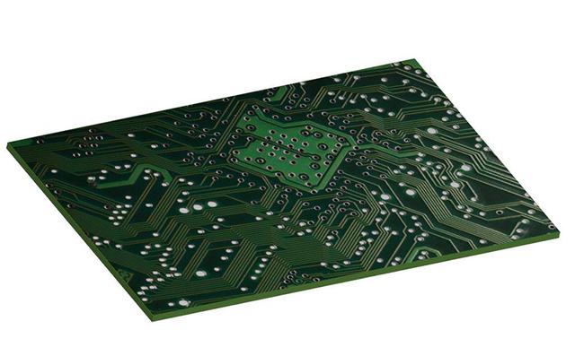
As a historical product in the 21st century, the single chip microcomputer successfully integrates the computer on a SMAll PCB, realizing the interconnection of all things and providing many conveniences for our life experience. Now Lao Chen will show you what ingenious designs are needed for the main control board of the microcontroller
In terms of the layout of components, the components related to each other should be placed as close as possible. For example, the clock generator, crystal oscillator, and CPU clock input are prone to generate noise, so they should be placed closer. For those devices, low current circuits, high current circuit switching circuits, etc. that are prone to generate noise, they should be as far away from the logic control circuit and storage circuit (ROM, RAM) of the microcontroller as possible. If possible, these circuits can be made into circuit boards separately, which is conducive to anti-interference and improves the reliability of the circuit.
2. Decoupling capacitor
Try to install decoupling capacitors beside key components, such as ROM, RAM and other chips. In fact, PCB wiring, pin wiring and wiring may have a large inductance effect. A large inductance may cause serious switching noise SPIkes on the Vcc wiring. The only way to prevent switching noise spikes on Vcc cabling is to place a 0.1uF electronic decoupling capacitor between the VCC and the power supply ground. If surface mount components are used on PCB board, chip capacitors can be used to directly cling to components and fixed on Vcc pins. It is better to use ceramIC chip capacitor because it has low electrostatic loss (ESL) and high frequency impedance. In addition, the dielectric stability of this capacitor in temperature and time is also very good. Tantalum capacitors should not be used as far as possible because of their high impedance at high frequencies.
Pay attention to the following points when placing decoupling capacitors:
(1) Connect an electrolytic capacitor of about 100uF across the power input terminal of the PCB. If the volume allows, it is better to have a larger capacitance.
(2) In principle, a 0.01uF ceramic chip capacitor should be placed beside each integrated circuit chip. If the gap of the circuit board is too small to be placed, a 1~10 tantalum capacitor can be placed around every 10 chips.
(3) For the components with weak anti-interference ability and large current change when turning off, RAM, ROM and other storage components, decoupling capacitors should be connected between the power line (Vcc) and the ground wire.
(4) The lead of capacitor shall not be too long, especially the high frequency bypass capacitor shall not have lead.
3. Ground wire design
In the microcontroller control system, there are many kinds of ground wires, such as systematic ground, shielding ground, logic ground, analog ground, etc. Whether the ground wire is reasonably arranged will determine the anti-interference ability of the circuit board. When designing ground wires and grounding points, the following issues should be considered:
(1) Logic ground and analog ground shall be wired separately and cannot be used together. Connect their respective ground wires to the corresponding power ground wires respectively. During the design, the analog ground wire shall be thickened as much as possible, and the grounding area of the leading out end shall be increased as much as possible. Generally speaking, it is better to isolate the input and output analog signals from the SCM circuit through optocouplers.
(2) When designing the printed circuit board of logic circuit, its ground wire shall form a closed loop form to improve the anti-interference ability of the circuit.
(3) The ground wire shall be as thick as possible. If the ground wire is very thin, the resistance of the ground wire will be large, causing the ground potential to change with the change of current, resulting in unstable signal level, and reducing the anti-interference ability of the circuit. If the wiring space allows, the width of the main ground wire shall be at least 2~3mm, and the ground wire on the component pin shall be about 1.5mm.
(4) Pay attention to the selection of grounding points. When the signal frequency on the circuit board is lower than 1MHz, since the electromagnetic induction between the wiring and the components has little influence, and the circulating current formed by the grounding circuit has great influence on the interference, one point grounding shall be adopted to prevent it from forming a loop. When the signal frequency on the circuit board is higher than 10MHz, the ground wire impedance becoMES large due to the obvious inductance effect of the wiring, and the circulating current formed by the grounding circuit is no longer the main problem. Therefore, multi-point grounding shall be adopted to minimize the ground wire impedance.
4. Others
(1) In addition to widening the wiring width as much as possible according to the size of current, the wiring of power lines and ground wires should be consistent with the wiring direction of data lines. At the end of the wiring work, ground wires should be used to pave the bottom of the circuit board where there is no wiring. These methods are helpful to enhance the anti-interference ability of the circuit.
(2) The width of the data line should be as wide as possible to reduce the impedance. The width of data line shall not be less than 0.3mm (12mil) at least. It is more ideal if 0.46~0.5mm (18mil~20mil) is used.
(3) Since a via of the circuit board will bring about a capacitance effect of about 10pF, which will introduce too much interference to high-frequency circuits, the number of vias should be reduced as much as possible during wiring. Moreover, too many vias will also reduce the mechanical strength of the circuit board.
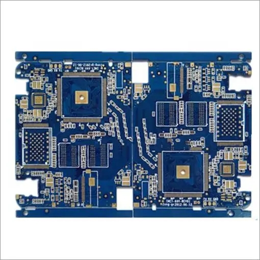
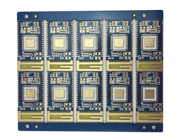
PCB manufacturing, PCB design, PCBA processing manufacturers will explain the design skills of single-chip PCB control board for you.


抖音二維碼

Q Q二維碼

微信二維碼
點擊
然后
聯系
然后
聯系
電話熱線
13410863085Q Q

微信

- 郵箱