鑫景福致力于滿足“快速服務,零缺陷,輔助研發”PCBA訂購單需求。


PCBA方案設計
How to optimize the electromagnetic compatibility (EMC) design of PCB
With the development of the electrICal era, there are more and more electromagnetic wave sources in human living environment, such as radio broadcasting, television, microwave communication, household appliances, power frequency electromagnetic fields and high-frequency electromagnetic fields of transmission lines. When the field strength of these electromagnetic fields exceeds a certain limit and the action time is long enough, it may endanger human health; It also interferes with other electronic equipment and communications. For this, protection is required. The concepts of electromagnetic interference and shielding are often put forward in the development, production and use of electronic products. During the normal operation of electronic products, the core is a coordinated working process between the PCB board and the components and parts instalLED on it. It is very important to improve the performance of electronic products and reduce the influence of electromagnetic interference.
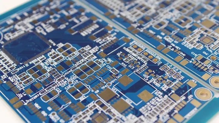
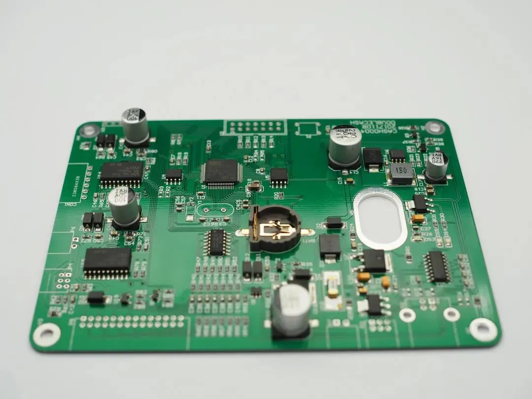
Printed Circuit Board (PCB) is the supporting part of circuit components and devices in electronic products. It provides the electrical connection between circuit components and devices. It is the most basic component of various electronic equipment. The performance of PCB is directly related to the quality and performance of electronic equipment. With the development of integrated circuit, SMT technology and micro assembly technology, there are more and more high-density and multi-functional electronic products, resulting in complex wire layout, various parts and components, and intensive installation on PCB, which will inevitably lead to more and more serious interference between them. Therefore, the suppression of electromagnetic interference has become the key to the normal operation of an electronic system. SIMilarly, with the development of electrical technology, the density of PCB is getting higher and higher. The quality of PCB design has a great impact on the interference and anti-interference ability of the circuit. In order to obtain the best performance of electronic circuits, in addition to the selection of components and circuit design, good PCB design is also a very important factor in electromagnetic compatibility (EMC).
1.1 Reasonable PCB layer design
According to the complexity of the circuit, reasonable selection of PCB layers can effectively reduce electromagnetic interference, significantly reduce PCB volume and the length of current loop and branch wiring, and significantly reduce cross interference between signals. The experiment shows that the noise of the four layer plate is 20dB lower than that of the double layer plate when the same material is used. However, the higher the number of layers, the more complex the manufacturing process, and the higher the manufacturing cost. In the multi-layer PCB board wiring, it is better to use a "well" shaped MESh wiring structure between adjacent layers, that is, the direction of each adjacent layer's wiring is perpendicular to each other. For example, the upper side of a PCB board is wired horizontally and the lower side is wired longitudinally, and then connected via holes.
1.2 Reasonable PCB board size design
When the size of PCB board is too large, it will lead to the growth of printed wire, the increase of impedance, the decline of noise resistance, and the increase of equipment volume and cost. If the size is too SMAll, the heat dissipation is poor, and adjacent lines are vulnerable to interference. In general, the mechanical layer determines the physical frame, that is, the overall dimensions of the PCB board, and the keepout layer determines the effective area of the layout and wiring. Generally, according to the number of functional units of the circuit, all components of the circuit are integrated, and the optimal shape and size of the PCB board are finally determined. Rectangle is usually selected, and the aspect ratio is 3:2. When the size of the circuit board surface is greater than 150mm * 200mm, the mechanical strength of the PCB board shall be considered.
2. Layout of PCB board
In PCB design, electronic engineers may only focus on improving the density, reducing the space occupation, making simple, or pursuing beautiful and even layout, ignoring the impact of circuit layout on electromagnetic compatibility (EMC), so that a large number of signals radiate into the space to form mutual interference. A poor PCB wiring can cause more electromagnetic compatibility (EMC) problems than eliminate them.
The layout and wiring characteristics of digital circuits, analog circuits and power supply circuits in electronic equipment are different, and their interference and interference suppression methods are different. Due to the different frequencies of high frequency and low frequency circuits, their interference and interference suppression methods are different. Therefore, digital circuit, analog circuit and power circuit should be placed separately in component layout, and high-frequency circuit and low-frequency circuit should be separated. If possible, separate them or make a PCB separately. In the layout, special attention shall be paid to the device distribution of strong and weak signals and the signal transmission direction.
2.1 Component layout of PCB
The layout of PCB components is the same as that of other logic circuits. The components related to each other should be placed as close as possible to achieve better noise resistance. Anti electromagnetic interference shall be fully considered for the position of components arranged on PCB board. One of the principles is to keep the lead wires between components as short as possible. In terms of layout, the analog signal part, high-speed digital circuit part and noise source part (such as relay, large current switch, etc.) shall be reasonably separated to minimize the signal coupling between them.
The clock generator, crystal oscillator and CPU clock input are easy to generate noise, so they should be close to each other. Devices, small current circuits, large current circuits, etc. that are easy to generate noise shall be as far away from logic circuits as possible. If possible, it is very important to make another PCB.
General layout requirements for PCB components: the layout of circuit components and signal paths must minimize the mutual coupling of unwanted signals.
1) The low-level signal channel shall not be close to the high-level signal channel and the power line without filtering, including the circuit that can generate transient process.
2) Separate low-level analog circuit and digital circuit to avoid common impedance coupling between analog circuit, digital circuit and power common circuit.
3) High, medium and low speed logic circuits use different areas on the PCB.
4) Arrange the circuit in such a way that the length of the signal line is minimum.
5) Ensure that there are no too long parallel signal lines between adjacent boards, between adjacent layers of the same board, or between adjacent wiring of the same layer.
6) The electromagnetic interference (EMI) filter shall be as close to the electromagnetic interference source as possible and placed on the same circuit board.
7) DC/DC converters, switching elements and rectifiers shall be placed as close to the transformer as possible to minimize their conductor lengths.
8) Place the voltage regulating element and filter capacitor as close as possible to the rectifier diode.
9) PCB boards are divided according to frequency and current switching characteristics, and the distance between noise components and non noise components is farther.
10) The wiring sensitive to noise shall not be parallel to the high current and high speed switching lines.
11) The element layout should also pay special attention to heat dissipation. For high-power circuits, those heating elements, such as power tubes and transformers, should be placed as close to the side as possible to facilitate heat dissipation. Do not concentrate in one place, nor do high capacitors too close to avoid premature aging of the electrolyte.
2.2 PCB wiring
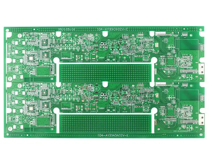
A PCB is composed of a series of multilayer structures with lamination, routing and pre impregnation on the vertical stack. In a multilayer PCB board, the signal line is laid on the outermost layer to facilitate debugging.
In the case of high frequency, the routing, via, resistance, capacitance, distributed inductance and distributed capacitance of connectors on the PCB cannot be ignored. Resistance will reflect and absorb high-frequency signals. The distributed capacitance of the wiring will also play a role. When the routing length is greater than 1/20 of the corresponding wavelength of the noise frequency, the antenna effect will be generated, and the noise will be transmitted outward through the routing.
Wire connection of PCB board is mostly completed through holes. One via can bring about 0.5pF distributed capacitance, and reducing the number of via can significantly improve the speed.
A 2-6 pF capacitor is introduced into the packaging material of an integrated circuit itself. A connector on a PCB board has 520nH distributed inductance. A dual in-line 24 pin integrated circuit socket with 4~18nH distributed inductance.
General requirements to avoid the influence of PCB wiring distribution parameters:
1) Increase the distance between wires to reduce the crosstalk of capacitive coupling.
2) When wiring with two panels, the conductors on both sides should be perpendicular, oblique, or bent to avoid being parallel to each other to reduce parasitic coupling; The printed wires used as the input and output of the circuit shall be kept away from adjacent parallels as far as possible to avoid feedback. It is better to add grounding wires between these wires.
3) The sensitive high-frequency lines are laid far away from the high noise power lines to reduce the coupling between them; The high frequency digital circuit is thinner and shorter.
4) Widen the power line and ground wire to reduce the impedance of the power line and ground wire.
5) Try to use 45 ° polylines instead of 90 ° polylines to reduce the external transmission and coupling of high-frequency signals.
6) For address lines or data lines, the difference in routing length should not be too large, or the short lines should be compensated by manual routing.
7) Large current signals, high voltage signals and small signals should be isolated (the isolation distance is related to the withstand voltage to be withstood. Generally, the distance on the board should be 2mm at 2kV, and it should be increased in proportion. For example, if the 3kV withstand voltage test is to be withstood, the distance between high and low voltage lines should be more than 3.5mm. In many cases, to avoid creepage, slots are also opened between high and low voltage on the PCB board).
3. Circuit Design in PCB
When designing electronic circuits, more attention is paid to the actual performance of the product, rather than to the electromagnetic compatibility (EMC) and electromagnetic interference (EMI) suppression and electromagnetic anti-interference characteristics of the product. In order to achieve the purpose of electromagnetic compatibility when using circuit schematic diagram for PCB layout, necessary measures must be taken, that is, necessary additional circuits must be added on the basis of its circuit schematic diagram to improve the electromagnetic compatibility of its products. The following circuit measures can be adopted in actual PCB design:
1) A resistor can be connected in series on the PCB wiring to reduce the jump rate of the lower edge of the control signal wire.
2) Try to provide some form of damping (high-frequency capacitor, reverse diode, etc.) for relays, etc.
3) The signal entering the PCB shall be filtered, and the signal from the high noise area to the low noise area shall also be filtered. At the same time, the serial terminal resistance shall be used to reduce the signal reflection.
4) The useless end of MCU shall be connected to power or ground through corresponding matching resistance, or defined as output end. The power and ground terminals on the integrated circuit shall be connected, and shall not be suspended.
5) The unused gate circuit input terminal shall not be suspended, but connected to the power supply or ground through the corresponding matching resistance. The positive input terminal of the idle operational amplifier is grounded, and the negative input terminal is connected to the output terminal.
6) A high-frequency decoupling capacitor is set for each integrated circuit. A small high-frequency bypass capacitor shall be added beside each electrolytic capacitor.
7) Use high-capacity tantalum capacitor or polyester capacitor instead of electrolytic capacitor as charging and discharging energy storage capacitor on PCB. When using tubular capacitors, the enclosure should be grounded.
PCB manufacturers, PCB designers and PCBA manufacturers will explain how to optimize the electromagnetic compatibility (EMC) design of PCBs.


抖音二維碼

Q Q二維碼

微信二維碼
點擊
然后
聯系
然后
聯系
電話熱線
13410863085Q Q

微信

- 郵箱