鑫景福致力于滿足“快速服務,零缺陷,輔助研發”PCBA訂購單需求。


PCBA方案設計

What is the cause of PCB failure
As the carrier of various components and the hub of circuit signal transmission, this PCB has become an important and key part of electronIC information products Its quality and reliability level determines the quality and reliability of the whole equipment With the miniaturization of electronic information products and the environmental requirements of lead-free and halogen-free, PCBs are also developing towards high-density, high Tg and environmental protection However, due to cost and scientific and technological reasons, a large number of failure problems occurred in the production and application of PCB s, which caused many quality disputes In or der to clarify this cause of the failure in or der
To find a solution to the problem and distinguish the responsibilities, it is necessary to analyze the faults that have occurred
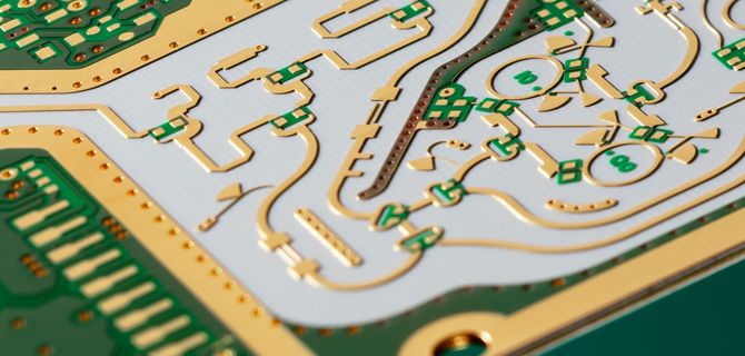
PCB board

Basic procedure of failure analysis
To observe the exact cause or mechanism of the failure or failure of the PCB, the basic principles and analysis process must be followed, otherwise valuable fault information may be lost, resulting in analysis unable to continue or incorrect conclusions may be drawn The general basic process is: first, based on the fault phenomenon, the fault location and fault mode must be determined through information collection, functional test, power performance test, and
SIMple visual inspection, that is, fault location or fault location For simple PCB or PCB A., the fault location is easy to determine, but for more complex BGA or MCM packaging devices or substrates, the defects are not easy
to observe through a microscope and are not easy to determine for a while. At this point, other means are needed Of course Then we need to analyze the failure mechanism, that is, use variable physical and chEMIcal methods to analyze the mechanism
That causes the failure or defect of the PCB, such as virtual welding, pollution, mechanical damage, water stress, medium corrosion, fatigue damage, CAF or ion migration, stress overload, etc Then, the cause of the failure is analyzed,
That is, based on the failure mechanism and process analysis, find the cause of the failure mechanism and conduct test verification if necessary Generally, the accurate cause of induced failure
can be found through test verification. This provides a targeted basis for further improvement, The fault analysis is based on the experimental data. The facts and conclusions obtained during the analysis are clear
Logical reasoning is strict Don't imagine it out of thin air In the analysis process, pay attention to the basic principle that the analysis method should be from simple to complex. From outside to inside, never
destroying the sample and then using it. Only in this way can we avoid the loss of key information and introduce new artificial failure mechanisms If the party involved in the accident destruction or escapes the
It is difficult for a wise policeman to determine the responsibility accurately At this time, the traffic law usually requires the person who escapes from the scene or the party who damages the scene to take full responsibility Fault analysis PCB or PCB A is the same If you use a soldering iron to repair the faiLED solder joints, or use a pair of scissors to cut the PCB strongly, then there is no way to start the analysis. The fault site has been damaged Especially when there are few failed samples, once the fault site environment is damaged or damaged, the real fault cause cannot be obtained
Failure Analysis Technology
Optical microscope: this optical microscope is mainly used for the appearance inspection of PCB boards to search for faulty parts and relevant physical evidence, and preliminarily judge PCB boards The appearance inspection
Mainly checks the PCB contamination, corrosion, location of broken boards, circuit wiring and fault rule. If it is batch or single, it is always concentrated in a certain area, etc X-ray (X-ray): For some parts that cannot be visually inspected, and PCB boards must be inspected with X-ray fluoroscopy system The X-ray fluoroscopy system uses different data thicknesses or different data densities for imaging according to different principles of X-ray moisture absorption or transmittance This technology is more used to check the position of solder joints of PCB A, internal defects of through-hole, and defective solder joints of high-density BGA or CSP devices
Slice analysis: Slice analysis is a process to obtain the cross section structure of PCB board through a series of methods and steps such as sampling, inlaying, slicing, polishing, corrosion and observation. Through slice analysis, we can obtain rich microstructure information (through-hole, electroplating, etc.) reflecting the quality of PCB, which provides a good basis for the next step of quality improvement. However, this method is destructive. Once sliced, the sample will inevitably be damaged.
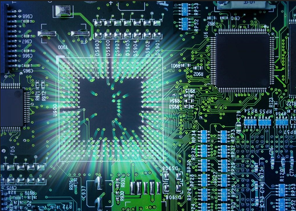
PCB board
Scanning acoustic microscope: At present, C-mode ultrasonic scanning acoustic microscope is mainly used for electronic packaging or assembly analysis It uses amplitude, phase and polarity changes caused by high-frequency ultrasonic reflection on discontinuous interfaces of data and images. Its scanning method is to scan the information in the XY plane along the Z-axis Therefore, the scanning acoustic microscope can be used to detect components, data,
As well as various defects inside PCB and PCB A, including cracks, delaminations, inclusions, and cavities If the scanning acoustic frequency width is sufficient, the internal defects of the solder joint can also be directly detected A typical
scanning acoustic image uses a red warning color to indicate the existence of defects. A large number of mobility reflow sensitivity issues are generated during
the conversion from lead to lead-free process. That is to say, when the lead-free process temperature is high, the moisture absorbing plastic packaging device will have internal or substrate delamination cracking during reflow, which is similar to the common PCB
will often burst at the high temperature of the lead-free process. At this time, the scanning acoustic microscope highlighted its special advantages in multi-layer high-density nondestructive testing PCB boards Generally, objective bursts
can be detected only by visual inspection of the appearance.
Micro infrared analysis: Micro infrared analysis is an analysis method combining infrared spectroscopy and microscope It uses the principle of different absorption of infrared spectrum by different fabrics (mainly organic matter) to analyze the
Compound composition of the material, combined with microscope, can make visible light and infrared light have the same optical path, as long as they are in the visible field of vision, it is possible to find trace organic pollutants to be
analyzed. Without the combination of microscopes, infrared spectroscopy usually can only analyze a large number of samples However, in many cases, in the field of electronic technology, micro pollution can lead to poor solvability of PCB
pads or lead pins. It can be imagined that without the infrared spectrum of the microscope, it is difficult to solve the process problem The main purpose of micro-infrared analysis is to analyze the organic contaminants on the welded surface or the
Surface of the solver joint, and analyze the cause of corrosion or poor solvability
Scanning electron microscope analysis: scanning electron microscope is a useful large-scale electron microscope imaging system for fault analysis It is usually used for topographic observation The current scanning electron microscope is already
Very powerful, any fine structure or surface feature can be magnified Observe and analyze hundreds of thousands of tiMES In fault analysis, scanning electron microscopy (SEM) is mainly used to analyze the failure mechanism of PCB or solder joint Specifically,
It is used to observe the topographical structure of the pad surface, the metallographic structure of the solder joint, and measure the intermetallic compound and solderability Coating analysis and tin whisker analysis and measurement Unlike an
Optical microscope, scanning electron microscope produces electronic images, so only black and white are produced The sample of scanning electron microscope needs conductivity Non-conductors and some semiconductors
need to be sprayed with gold or carbon. Otherwise, the accumulation of surface charge of the sample will affect the observation of the sample In addition, the image of the scanning electron microscope is more profound than the field depth of the optical microscope. It is an important analysis method for inhomogeneous samples such as metallography, micro fracture and tin whisker
Thermal analysis: Differential Scanning Calorimeter (DSC)
Differential Scanning Calorimetry (Differential Scanning Calorimetry) is a method to measure the relationship between the power difference between the input material and the reference material and the temperature (or time) under program
temperature control. This is an analytical method for studying the relationship between heat and temperature Based on this relationship, physics can study and analyze the chemical and thermodynamic properties of data DSC has a
Wide range of applications, but in the analysis of PCB boards, it is mainly used to measure the curing degree and glass transition temperature of various polymer materials used on the surface of PCB boards These two parameters determine the reliability of
The PCB is in the subsequent process


抖音二維碼

Q Q二維碼

微信二維碼
點擊
然后
聯系
然后
聯系
電話熱線
13410863085Q Q

微信

- 郵箱