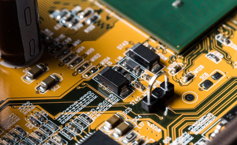

Laser processing technology in PCB manufacturing
Versatile electronIC products to printed circuit board (PCB) Closely interconnect multiple components in a limited area and stabilize the circuit circuit boards are getting denser and denser For example, the opening and line width are further reduced, the distance and accuracy between them are continuously improved, and the diameter depth ratio is continuously improved The number of circuit layers can reach more than 10 The number of micropores in the same layer is greater than 50000, but the spacing should be less than 0.05 mm, and the aperture should be less than 150 mm It is difficult to overcome the problem of drilling data, cooling, chip removal, and machining positioning when drilling PCBmechanically The application of laser processing can better meet the quality requirements
PCB board

1. Application of laser beam
The high-density PCB manufactured by iPCB is a multi-layer structure composed of insulating resin and glass fiber materials, with the middle conductive layer. They are then laminated and combined. The principle of laser processing is to focus the laser beam on the surface of the printed circuit board, so that the data can be instantly melted and evaporated, forming holes. Since copper and resin are two different materials, the melting temperature of copper foil is 1084 ° C, while that of insulating resin is only 200-300 ° C. In this case, when laser drilling is used, parameters such as beam wavelength, mode, diameter and pulse must be reasonably selected and controlLED.
1.1 Influence of beam wavelength and mode on processing
When drilling, the laser first processes copper foil, and the absorption of copper to laser increases with the increase of wavelength For example, the absorption of CO2 laser with wavelength of 9 is as high as 351 to 355 m from 4 to 10.6 mm, while the absorption of YAG/UV laser is as high as 70%, compared with 0.15% You can use YAG/UV laser or conformal mask method to drill holes on traditional printed boards In order to improve the integration of high-density PCB, each layer of copper foil is only 18m long, and the resin extract under the copper foil has a high absorption rate of carbon dioxide laser (about 82%), which is the condition of application Provide CO2 laser drilling The photoelectric conversion rate and processing efficiency of the carbon dioxide laser are much higher than those of the YAG laser/UV laser. In this regard, as long as there is enough beam energy and the copper foil is processed to improve the laser absorption, the carbon dioxide laser PCB can be opened directly
The transverse mode of laser beam has great influence on the divergence angle and energy output of laser beam To obtain enough beam energy, it is necessary to establish a suitable beam output mode The ideal state is to form a lower Gaussian mode output This allows for very high energy density This provides a prerequisite for the beam to be well focused on the lens Low order modes can be obtained by changing resonator parameters or installing diaphragm Installing the diaphragm will reduce the beam energy output, but it can limit and assist the high mode laser to participate in drilling Improve the roundness of the SMAll hole
1.2 Effect of beam pulses
Multi pulse laser is used for drilling. The output density of pulse laser must at least reach the evaporation temperature of copper foil. After the copper foil is burned, the energy of the single pulse laser is weakened, and the bottom substrate cannot be effectively ablated to form a through-hole. However, if the energy is too high, it is necessary to ensure that the beam energy is not too high when drilling. After the copper foil is penetrated, the circuit board is excessively ablated and cannot be used for post-processing of the circuit board. The slightly tapered hole formed by micropores is ideal, which is very useful for the subsequent copper coating process.
2. Laser beam effect
Because the data characteristics of copper foil and substrate are very different, the interaction between laser beam and circuit board data has different effects, which has a significant impact on the aperture, depth and type of micropores.
2.1 Laser reflection and absorption
When the incident laser is first reflected and absorbed by the surface copper foil, the interaction between the laser and PCB begins. Copper foil has low absorption rate for infrared wavelength CO2 laser, and is difficult to process with high efficiency. Very low. The absorbed light energy increases the free electron kinetic energy of the copper foil material, most of which is converted into the thermal energy of the copper foil through the interaction between electrons and lattice or ions. This shows that, while improving the beam quality, the copper foil surface also needs to be pretreated. The copper foil surface can be coated with a layer of materials to enhance the light absorption, so as to improve the laser absorption.
2.2 Effect of beam effect
In laser processing, the copper foil is heated and evaporated when the light shines on it Therefore, the steam temperature is high, and it is easy to decompose and ionize. Photoelectric plasma is generated by light excitation Photoinduced plasma is usually a material vapor plasma When the energy transmitted by the plasma to the workpiece is greater than the light energy lost by the workpiece due to absorption of the plasma On the contrary, plasma enhances the absorption of laser energy by the workpiece Otherwise, the plasma will block the laser and reduce the laser absorption of the workpiece For carbon dioxide lasers, light induced plasma can increase the absorption of copper foil However, when the beam passes through, too much plasma will be refracted, thus affecting the hole positioning accuracy In general, the laser power density should be controlled at a reasonable value below 107W/cm2 to better control the plasma
In the laser drilling process, the pinhole effect plays a very important role in the absorption of newly added light energy Even if the copper foil is burnt, the laser will continue to ablate the substrate The substrate absorbs a lot of light energy, evaporates and expands violently, The pressure generated is: throw out the melted data to form a small hole The hole is also full of photoplasma, and the laser energy entering the hole is almost completely absorbed by the multiple reflection of the hole wall and the role of plasma Plasma absorption reduces the laser power density from the crater to the bottom of the crater Laser power density at the bottom of the pit is critical to generating a specific vaporization pressure to maintain a specific depth A small hole that determines the penetration depth during processing
3. Conclusion
The application of laser processing technology can greatly improve the drilling efficiency of high-density PCB micropores Experiences show (1) Combining numerical control technology, more than 30 openings of printed circuit board can be processed, with 000 micropores per minute Between 75 and 100 (2) Through the application of ultraviolet laser, the opening can be further reduced to less than 50mm, creating conditions for further expanding the use space of PCB
然后
聯(lián)系
電話熱線
13410863085Q Q

微信

- 郵箱


