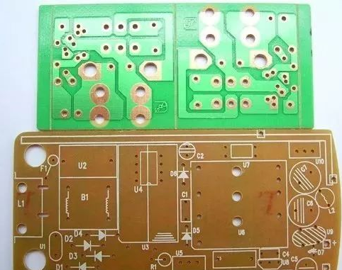
鑫景福致力于滿足“快速服務,零缺陷,輔助研發(fā)”PCBA訂購單需求。


PCBA方案設計
DetaiLED explanation of SIMple shortcut method for PCB routing constraint
PCB manufacturers, PCB designers and PCBA manufacturers will explain the simple and shortcut methods of PCB wiring constraints.
2、 Route constraints
Routing constraints: layer distribution routing constraints: layer distribution
The laminated structure of RF boards
1. Routing constraints: basIC requirements
1) The routing shall be as short as possible, without closed loop, acute angle and right angle. The line width shall be consistent, without floating line.
2) Differential signal lines are generally high-speed signals, which should meet the impedance symmetry. Differential lines cannot be crossed, and the difference in line length cannot exceed 100mil. The impedance requirements should be met between differential lines and between a single differential line and the ground. The number of differential wiring vias shall not exceed 4, and the spacing between differential wire pairs shall meet the 3W rule.
3) General crystal oscillator, pll filter device, analog processing signal processing chip, inductor, clock line, control line and electromagnetic sensitive line under the transformer.
4) Analog signals and digital signals, power lines and control signal lines, weak signals and any other signals cannot be routed side by side, and should be layered (preferably isolated from the ground) or distant. If cross routing is required between lines of adjacent layers, parallel routing is not allowed. In order to reduce the crosstalk between lines, ensure that the line spacing is large enough. When the line center spacing is not less than 3 tiMES the line width, 70% of the electric fields can be kept from interfering with each other, which is called the 3W rule. If 98% electric fields do not interfere with each other, 10W spacing can be used. (Note: When wiring the clock, pay attention to the effective isolation from the data line and control signal line. The farther the distance is, the better. Try not to lay it on the same layer.)
5) Strong radiation signal line (high frequency, high speed, especially clock line) shall not be close to the interface, handle bar, etc. to prevent external radiation.
6) Sensitive signal (mainly refers to weak signal, reset signal, input signal of comparator, reference power supply of AD, phase-locked loop filtering signal, filtering part of PLL circuit inside the chip) The wiring should be as short as possible, not close to the strong radiation signal, not placed at the edge of the board, and more than 15mm away from the external metal frame. For long distance wiring, it is allowed to wrap the ground (it should be noted that wrapping the ground may cause impedance changes) and inner layer wiring. In addition, for the routing of the chip with weak ESD, it is recommended to route the inner layer to reduce the probability of chip damage.
2. Routing constraints: power
1) Pay attention to power decoupling and filtering to prevent interference from different units through power lines. During power wiring, power lines shall be isolated from each other. The power line shall be isolated from other strong interference lines (such as CLK) with ground wire.
2) The power wiring of SMAll signal amplifier needs to be isolated by grounding copper sheet and grounding via to prevent other EMI interference from entering, thus deteriorating the signal quality of this level.
3) Different power supply layers should avoid overlapping in space. It is mainly to reduce the interference between different power sources, especially between some power sources with large voltage difference. The overlapping problem of power plane must be avoided. If it is difficult to avoid, the interlayer can be considered.
3. Wiring constraints: power overcurrent capability
1) The number of vias of the conductor printed wire of the power supply part transferred between layers meets the requirements of passing current (1A/ Ф 0.3mm hole)
2) The copper foil size of the POWER part of the PCB shall conform to the maximum current flowing through it, and allowance shall be taken into account (generally referred to as 1A/mm line width)
4. Routing constraints: grounding methods
1) The grounding wire shall be short and straight to reduce the distributed inductance and the interference generated by the common ground impedance.
Adjust the direction of filter capacitors in each group to narrow the ground circuit. As shown in Figure 15, the grounding of the three filter capacitors is biased to the relevant RF device direction, especially the high-frequency filter capacitor.
2) When the grounding device and power filter capacitor on the RF main signal path need to be grounded, it is required to be grounded nearby to reduce the grounding inductance of the device.
3) The bottom of some components is a grounded metal shell, so some grounding holes should be added in the projection area of the components, and the surface layer in the projection area should not be arranged with signal lines and through holes;
4) When the grounding wire needs to travel a certain distance, the line width shall be thickened and the line length shall be shortened. It is prohibited to approach or exceed 1/4 of the pilot wavelength to prevent signal radiation caused by antenna effect;
5) Except for special purposes, there shall be no isolated copper sheet, and the copper sheet must be provided with ground wire through holes
6) Some sensitive circuits and circuits with strong radiation sources are placed in shielding cavities, which are pressed on the surface of PCB during assembly. The PCB shall be designed with a "via shield wall", that is, a grounded via shall be added at the position close to the shield cavity wall on the PCB., There should be more than two rows of vias. The two rows of vias should be staggered, and the spacing of vias in the same row should be about 100mils.
5. Route constraints: general rules
1) The RF signal is applied to the top layer of PCB, and the plane layer below the RF signal must be a complete grounding plane to form a microstrip line structure.. To ensure the structural integrity of the microstrip line, it must be achieved that: the microstrip line in the same layer should be covered with copper sheet, and it is recommended that the edge of the copper sheet be 3H wide from the edge of the microstrip line. H is the thickness of the medium layer. No other signal through hole is allowed within 3H. RF signal routing is prohibited to cross the ground plane gap on the second floor. Ground copper sheet shall be added between uncoupled microstrip lines, and ground via shall be added on the ground copper sheet.
The distance between the microstrip line and the shielding wall shall be more than 3H. The microstrip line shall not cross the dividing line of the second floor ground plane.
2) It is required that the interval between ground copper sheet and signal wiring shall be ≥ 3H.
3) Ground wire holes shall be added at the edge of the ground copper sheet, and the hole spacing shall be about 100mils, which shall be evenly and orderly arranged;
4) The edge of ground wire copper sheet shall be smooth and flat, and no sharp burrs are allowed;
5) If there are other RF signal lines around the RF signal wiring, the grounding copper sheet shall be supplemented between them, and a grounding via shall be added on the grounding copper sheet at an interval of about 100mils to isolate.
6) If there are other irrelevant non RF signals (such as passing power lines) around the RF signal wiring, auxiliary grounding copper sheet shall be provided between them, and a grounding via shall be added every 100mils or so.
7) The RF signal vias are close to other wiring in the inner layer. As shown in the left figure, the passing power line is close to the RF signal vias. The EMI interference on the power line will enter the RF wiring. Therefore, the correct wiring method shown in the right figure of Figure 14 should be used to supplement the ground and add the ground vias between the power line and the RF signal vias for isolation. Sometimes the RF signal line in the inner layer is close to the vias of other signals with strong interference (such as passing power lines), and the same method is used to assist grounding and add grounding vias.
8) When the device mounting hole is a non-metallic hole, the RF signal wiring shall be far away from the device mounting hole. The grounding copper sheet shall be added between the RF signal wiring and the installation hole, and the grounding through hole shall be added.
PCB manufacturers, PCB designers and PCBA manufacturers will explain the simple and shortcut methods of PCB wiring constraints.


抖音二維碼

Q Q二維碼

微信二維碼
點擊
然后
聯(lián)系
然后
聯(lián)系
電話熱線
13410863085Q Q

微信

- 郵箱