鑫景福致力于滿足“快速服務(wù),零缺陷,輔助研發(fā)”P(pán)CBA訂購(gòu)單需求。


PCBA方案設(shè)計(jì)
Introduction to shortcut method of wiring in PCB design
1、 Wiring
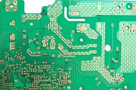
In PCB design, wiring is an important step to complete product design. It can be said that the previous preparations are all done for it. In the whole PCB, the wiring design process is the most limited, the most detaiLED and the largest workload.
PCB wiring includes single-sided wiring, double-sided wiring and multi-layer wiring. There are also two ways of wiring: automatIC wiring and interactive wiring. Before automatic wiring, wires with strict requirements can be wired interactively in advance. The side lines of input and output terminals should avoid adjacent parallelism to avoid reflective interference. If necessary, ground wires shall be added for isolation, and the wiring of two adjacent layers shall be perpendicular to each other, which may cause parasitic coupling.
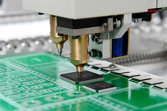
The routing rate of automatic routing depends on good layout, and the routing rules can be preset, including the bending tiMES of routing, the number of through holes, the number of steps, etc. Generally, the exploratory warp routing is carried out first to quickly connect the short lines, and then the maze routing is carried out. First, the global routing path optimization is carried out for the lines to be laid, which can disconnect the already laid lines as needed. And try to rewire to improve the overall effect.
I feel that the through-hole is not suitable for the current high-density PCB design. It wastes many valuable wiring channels. To solve this contradiction, blind hole and buried hole technologies have emerged. It not only completes the role of the through-hole, but also saves many wiring channels to make the wiring process more convenient, smooth, and perfect. The PCB design process is a complex and SIMple process. If you want to master it well, It also needs the majority of electronic engineering designers to experience themselves to get the true meaning.
1. Treatment of power supply and ground wire
Even though the wiring in the whole PCB board is well completed, the interference caused by improper consideration of power supply and ground wire will degrade the performance of the product, and sometimes even affect the success rate of the product. Therefore, the wiring of electrical and ground wires should be taken seriously to minimize the noise interference generated by electrical and ground wires to ensure the quality of products.
Every engineer engaged in electronic product design knows the cause of the noise between the ground wire and the power line, and now only describes the reduced noise suppression:
·It is well known that a coupling capacitor is added between the power supply and the ground wire.
·Widen the width of power supply and ground wire as much as possible. The ground wire is better than the power wire. Their relationship is: ground wire>power wire>signal wire. Generally, the width of signal wire is 0.2 ~ 0.3mm, the narrowest width can reach 0.05 ~ 0.07mm, and the power wire is 1.2 ~ 2.5mm
The PCB of digital circuit can be used to form a loop with a wide ground wire, that is, to form a ground grid for use (the ground of analog circuit cannot be used in this way)
·Use a large area of copper layer as the ground wire, and connect all unused places on the printed board with the ground as the ground wire. Or it can be made into multilayer boards, with one layer for power supply and one layer for ground wire.
2. Common Ground Processing of Digital Circuit and Analog Circuit
Nowadays, many PCBs are no longer single functional circuits (digital or analog circuits), but are composed of digital circuits and analog circuits. Therefore, when wiring, it is necessary to consider the mutual interference between them, especially the noise interference on the ground wire.
The frequency of digital circuit is high and the sensitivity of analog circuit is strong. For the signal line, the high-frequency signal line is as far away from the sensitive analog circuit device as possible. For the ground wire, the integrated PCB has only one node to the outside world. Therefore, the problem of digital and analog common ground must be handled inside the PCB. In fact, the digital ground and analog ground inside the board are not connected with each other, Only at the interface between PCB and the outside world (such as plug).
There is a short circuit between digital ground and analog ground. Please note that there is only one connection point. Some are not common on PCB, which is determined by system design.
3. The signal line is laid on the electrical (ground) layer
When wiring multilayer printed circuit boards, there are not many wires left in the signal line layer, and the additional layers will cause waste and increase the workload and cost of production. To solve this contradiction, wiring on the electrical (ground) layer can be considered.
The power layer should be considered first, and then the stratum. Because it is better to preserve the integrity of the stratum.
4. Treatment of connecting leg in large area conductor
In large-area grounding (electricity), the legs of commonly used components and parts are connected with each other, and the treatment of the connecting legs needs to be considered comprehensively. As far as electrical performance is concerned, it is better to fully connect the bonding pad of the component leg with the copper surface, but there are some hidden dangers in the welding and assembly of components, such as:
·High power heater is required for welding.
·It is easy to cause false solder joints. Therefore, taking into account the electrical performance and process needs, it is made into cruciform pads, which are called heat shields, commonly known as thermal pads,
In this way, the possibility of false welding points due to excessive heat dissipation of the section during welding can be greatly reduced. The treatment of the electric (grounding) leg of the Multilayer board is the same.
5. The role of network system in cabling
In many CAD systems, routing is determined by the network system. The grid is too dense, the access is increased, but the step size is too SMAll, and the amount of data in the map field is too large, which inevitably requires higher storage space of the equipment, and has a great impact on the operation speed of computer electronic products.
However, some channels are invalid, such as those occupied by the pad of the component leg or by the mounting hole or the fixing hole. Too sparse grid and too few paths have a great impact on the deployment rate. Therefore, it is necessary to have a reasonably dense grid system to support the routing.
The distance between the legs of standard components is 0.1 inch (2.54mm), so the foundation of the grid system is generally 0.1 inch (2.54 mm) or an integral multiple of less than 0.1 inch, such as 0.05 inch, 0.025 inch, 0.02 inch, etc.
6. Design Rule Check (DRC)
After the wiring design is completed, it is necessary to carefully check whether the wiring design conforms to the rules formulated by the designer, and also to confirm whether the rules formulated conform to the requirements of the PCB production process. Generally, the following aspects are checked:
·Whether the distance between line and line, line and component pad, line and through-hole, component pad and through-hole, through-hole and through-hole is reasonable and meets Production requirements.
·Whether the width of power line and ground wire is appropriate, and whether the power line and ground wire are tightly coupled (low wave impedance)? Is there any place in the PCB where the ground wire can be widened.
·Whether the best measures have been taken for the key signal lines, such as the shortest length, adding protective lines, and the input lines and output lines are obviously separated.
·Whether the analog circuit and digital circuit have their own independent ground wires.
·Whether the graphics (such as icons and labels) added in the PCB will cause signal short circuit.
·Modify some undesirable alignments.
·Is there a process line on the PCB? Whether the resistance welding meets the requirements of the production process, whether the resistance welding size is appropriate, and whether the character MARK is pressed on the device pad to avoid affecting the electrical installation quality.
·Whether the frame edge of the power supply layer in the multilayer board is shrunk, for example, the copper foil of the power supply layer is exposed outside the board, which is easy to cause short circuit.
7. Check whether there are acute angles, impedance discontinuities, etc
1) For high-frequency current, when the bend of the wire presents a right angle or even an acute angle, the magnetic flux density and electric field intensity near the bend are relatively high, which will radiate strong electromagnetic waves, and the inductance here will be relatively large, so the inductance will be larger than the obtuse angle or rounded corner.
2) For the bus wiring of digital circuits, the wiring turns show obtuse angles or rounded corners, and the area occupied by wiring is relatively small. Under the condition of the same line spacing, the width of the total line spacing is 0.3 times less than that of the right angle turn.
8. Check 3W and 3H principles
1) The clock, reset, signals above 100M, and some key bus signals must meet the 3W principle with other signal lines. The same layer and adjacent layers have no longer parallel lines, and the number of vias on the link is as small as possible.
2) There is a problem with the number of vias for high-speed signals. Some device instructions generally have strict requirements on the number of vias for high-speed signals. The principle of consulting the interconnection is that except for the necessary pin fanout vias, it is strictly prohibited to make redundant vias in the inner layer. They have laid the 8G PCIE 3.0 wiring and also made 4 vias, which is no problem.
3) The center distance between clocks and high-speed signals on the same floor shall strictly meet 3H (H is the distance from the routing floor to the return plane); The signals of adjacent layers are strictly prohibited to overlap, and it is suggested that the principle of 3H should also be met. There are tools available to check the above crosstalk problems.
The Circuit board manufacturer, circuit board designer and PCBA manufacturer will explain the shortcut method of wiring in circuit board design.


抖音二維碼

Q Q二維碼

微信二維碼
點(diǎn)擊
然后
聯(lián)系
然后
聯(lián)系
電話熱線
13410863085Q Q

微信

- 郵箱