鑫景福致力于滿足“快速服務,零缺陷,輔助研發”PCBA訂購單需求。


PCBA方案設計
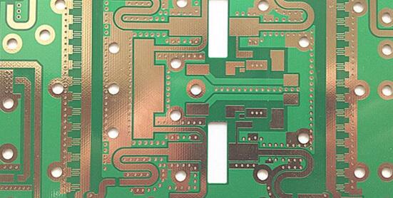
The Printed Circuit Board (PCB) is the heart of electronICs. They provide the conductive pathways that allow all electronIC components to function and connect. Multilayer PCBs are used to connect complex Electronic devices.
When copper is plated over holes, holes are created in the PCB to make electrical connections between layers. These holes are calLED through holes (plated through holes). According to its diameter, the pores can be classified as micropores.
What are micropores?
According to the printed circuit board Association, a microvia is any hole drilled in a PCB with a 1:1 aspect ratio and no larger than 0.010 inches. IPC used to consider microvias based on their size if they were SMAller than 0.006 inches. As technology improves, lasers can drill these tiny holes more frequently.
The IPC adopted a 1:1 aspect ratio definition of micropores to prevent changes in meaning. Microvias, also known as uVias or microwires, can be used to connect layers within a PCB. They are usually limited to connecting two layers at a time.
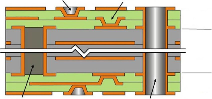
A diagram showing what a micropore is

Different types of micropores
PCB designers have many options when it coMES to drilling microvias. Each microwell is the same size. Their location is the main difference.
Blind Hole - Drilled to allow connection between the surface and the inner layer. These holes are not as deep as vias, but only reach one side of the PCB.
Buried microvias are holes in the inner layers of the PCB that do not reach the surface of the board.
Stacked vias - Several blind or buried vias are stacked on top of each other to allow connection of inner layers.
Staggered microvias are multiple layers of buried microvias. These micropores do not stack on top of each other. Instead, they are placed offset.
Via In-Pad Microvias are a method of placing microvias directly on copper pads. This allows the PCB to be miniaturized.
Diagram showing pore type

Advantages of Microvias in PCB Design
PCB designers can use microvias for circuit board design. Microvias provide thermomechanical reliability for function and performance. The ability to make via-in-pad microvias allows board miniaturization. Because micro-vias are smaller than standard through-holes or plated through-holes, they save space on the circuit board. You don't need a bigger board to hold all the components.
Microvias can be used to minimize defects in PCB designs. Lasers are used for drilling. Because of the shorter trace lengths of microvias, there are fewer manufacturing issues. Microvias have a significant impact on signal integrity when creating HDI boards. Higher radiation levels can be produced by using larger vias for high-speed circuits. Microvias can enhance RF capability and EMC properties. Microvias are more reliable than other types of vias and vias.
design with Microvias
There are many aspects to drilling microvias for PCBs. When designing the board, make sure that the vias do not exceed a 1:1 aspect ratio. Although drilling can be done at a higher rate, it is not reliable and is likely to cause plating defects. Regardless of aspect ratio, our PCB designers will never go below 4 mil diameter. When drilling into copper with a laser drill, the PCB design must not contain more than 1/2 ounce of copper. Lasers are more efficient at drilling and ablating copper below the copper surface, but the thickness of the copper increases.
If it is to be placed in multiple layers, there must be an additional lamination step for each layer that receives vias. If you don't plan to use the holes, you can fill them with a non-conductive material or close them by electroplating. Micropores may not need to be filled because they are so small. Electroplating is done in copper, a special bath used to create chEMIcals. This process allows the manufacturer to be more flexible in his design process.
If one layer is removed, such as a blind microvia moving from one layer to another, a gap will need to be left along the second pass-through layer. If you need to connect the second layer to the first, you can use microvias that can be stacked or staggered. However, staggered vias are easier to manufacture and offer higher reliability.
in conclusion
Since microvias allow PCB designers more flexibility in the manufacturing process, customers can connect multiple layers with higher reliability. Microbore drilling is more compatible with certain materials.
Talking to the PCB manufacturer before choosing a material set will give you a thorough understanding of your options. 911EDA engineers excel at helping customers select the right material for their application and connect your electrical components. You can also reduce material costs by using micro-drilling. Through holes can reduce the size of the circuit board and save space. PCBs manufactured with low manufacturing defects and risks can result in significant cost savings.
What are the test points in PCB design?
06-20,2022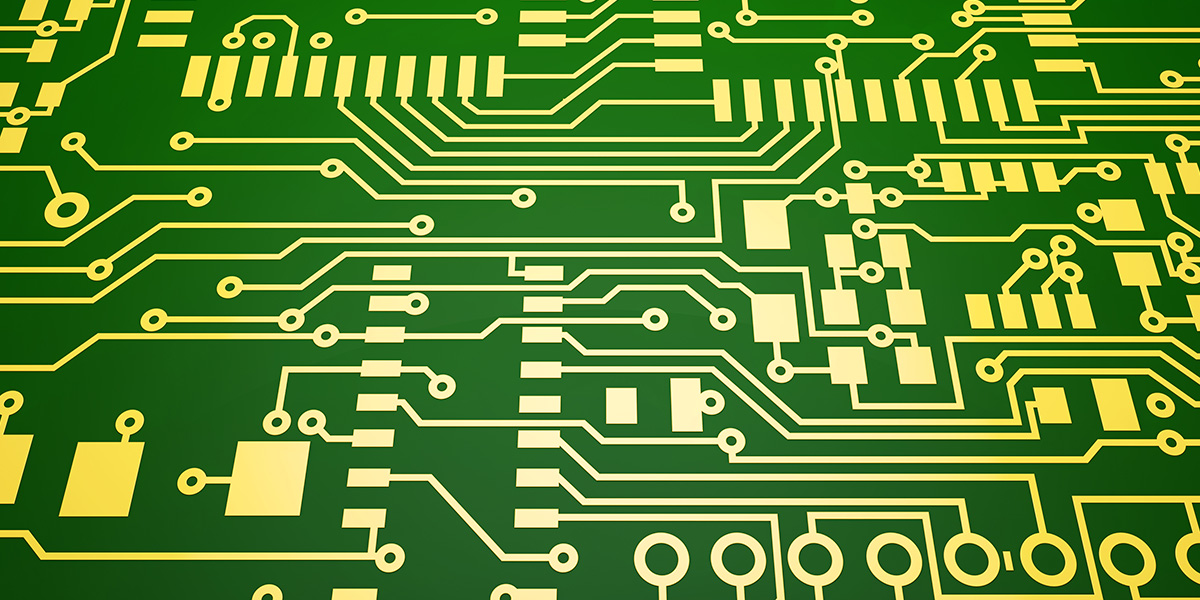


抖音二維碼

Q Q二維碼

微信二維碼
點擊
然后
聯系
然后
聯系
電話熱線
13410863085Q Q

微信

- 郵箱