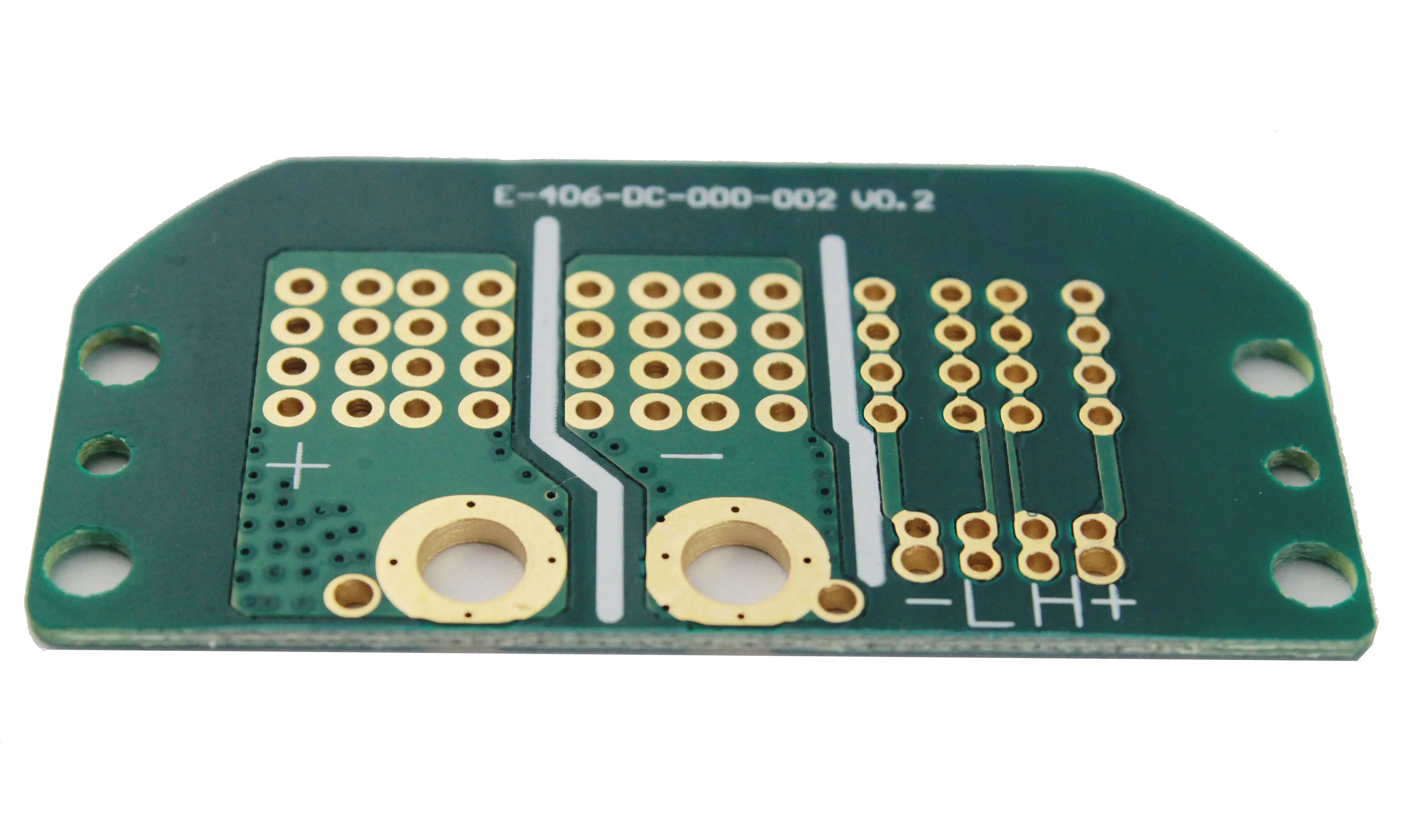
鑫景福致力于滿足“快速服務,零缺陷,輔助研發”PCBA訂購單需求。


PCBA方案設計
Common peripheral circuit design, hardware circuit design reference
circuit board manufacturers, circuit board designers and PCBA manufacturers will explain common peripheral circuit design and hardware circuit design reference
I have been engaged in the embedded industry for seven or eight years. Here I would like to share some hardware circuit design scheMES and experiences for some friends who have just learned embedded technology. Please ignore Dashen and Laoniao.
1、 Common design reference of key circuit
1. The R1 pull-up resistor clamps the uncertain signal to the high level through a resistor and maintains it in the non triggered state or returns to the original state after triggering. (Personal suggestion added)
2. C1 capacitor reduces key jitter and high-frequency signal interference. (Personal suggestion added)
3. R2 current limiting resistance (the value varies from 100 Ω to 10k. If internal pull-up is set, the value should not be too large, otherwise the current is not enough to pull down the IO port) protects the IO port from being burned by over-current and over-voltage, whICh can absorb static electricity or some high-voltage pulses. (Personal suggestion added)
4. D1ESD diode static protection diode to prevent static interference or damage to IO port. (This is added or not according to the cost and protection level requirements of PCB)
2、 External signal input design reference (SIMilar to the key)
1. The R3 pull-up resistor clamps the uncertain signal to the high level through a resistor and maintains it in the non triggered state or returns to the original state after triggering. (If the external connection line is relatively long and the internal pull-up capability of the chip is relatively weak, it is recommended to add it. Usually, the communication distance is not long, and the internal pull-up can be omitted.)
2. C2 capacitor prevents high-frequency signal interference. (Note that if the input frequency signal is relatively large, the C2 capacity should be reduced correspondingly, or C2 should be omitted directly)
3. R4 current limiting resistor protects the IO port from being burnt by over-current and over-voltage, which can absorb static electricity or some high-voltage pulses. (Personal suggestion added)
4. D2ESD diode static protection diode to prevent static interference or damage to IO port. (This is added or not according to the cost and protection level requirements of PCB)
3、 Output circuit relay design reference
1. U1 optocoupler separates high and low voltage to prevent high voltage interference and achieve electrical isolation
2. D5 1N4148 freewheeling diode bai protects the element from being punctured or burned by the induced voltage, connects the two ends of the element generating the induced electromotive force in parallel, and forms a loop with it, so that the high electromotive force generated by it is consumed in the loop in the form of freewheeling current, thus protecting the element in the circuit from damage.
4、 Darlington transistor design reference
Darlington transistors are commonly used by kids to drive stepping motors. In fact, they can be used for motor speed regulation, high-power switching circuits, driving relays, and driving LED light sources with high power. PWM is used to adjust brightness.
1. The R6 R7 R8 resistor is used for current limiting to prevent ULN2001 from being damaged, which may lead to the high voltage being directly input to the IO of MCU (since ULN2001D itself has a 2.7K resistor, R6 R7 R8 here can be omitted. If some driver chips do not have a resistor, it is better to add it by yourself. See the data manual of the selected chip for details)
2. COM terminal power supply When the output terminal is connected to an inductive load, the load does not need to add a freewheeling diode. There is a diode designed inside the chip, and only the COM port can be connected to the load power supply. When connecting to other loads, the COM port can not be connected.
3. When the resistance capacitance step-down circuit is used to supply power to ULN2001D, because the resistance capacitance step-down voltage cannot prevent the transient high-voltage fluctuation on the grid, a 104 capacitor must be connected to the COM terminal and the ground terminal of ULN2001D nearby. In other applications, this capacitor may not be added.
5、 Operational amplifier design reference
The current of the load is collected ingeniously by the application of the operational amplifier, which can accurately know the current load operation and whether it works normally. It is very easy to use. There are many wonderful and practical circuits in the operational amplifier, which will be shared with you one by one in the future. You can also search some classic circuits of the operational amplifier online when you are free.
1. GND2 is the ground terminal of the load, which is connected to the common ground through R16 resistance (larger power shall be selected for R16 according to the load current), and there will be a SMAll voltage difference
2. This circuit is an in-phase proportional operation circuit, so the voltage at the sampling terminal=input terminal voltage * (1+R9/R11)=69 times the input voltage. You can modify R9 to adjust the magnification according to the measurement range.
6、 MOS tube design reference application (control power output on/off)
7、 Input power design reference
Application If the circuit cost is tight, components can be appropriately deleted as needed
1. F1 self recovery fuse, over-current protection, the threshold value can be adjusted according to the actual load current.
2. D10 Schottky diode reduces the influence of the rear power supply on the front stage, prevents the reverse connection of the positive and negative power supply from burning out the rear stage circuit, and prevents the current from flowing back when the power supply is turned off. However, there is a voltage drop of about 0.4V across the diode. It is necessary to consider whether the voltage drop after 0.4V voltage drop will be lower than the normal working voltage of the rear stage circuit.
3. TVS tube input voltage over protection, generally 1.4 times of normal input voltage.
PCB manufacturers, PCB designers and PCBA manufacturers will explain common peripheral circuit design and hardware circuit design for reference.


抖音二維碼

Q Q二維碼

微信二維碼
點擊
然后
聯系
然后
聯系
電話熱線
13410863085Q Q

微信

- 郵箱